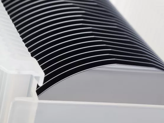
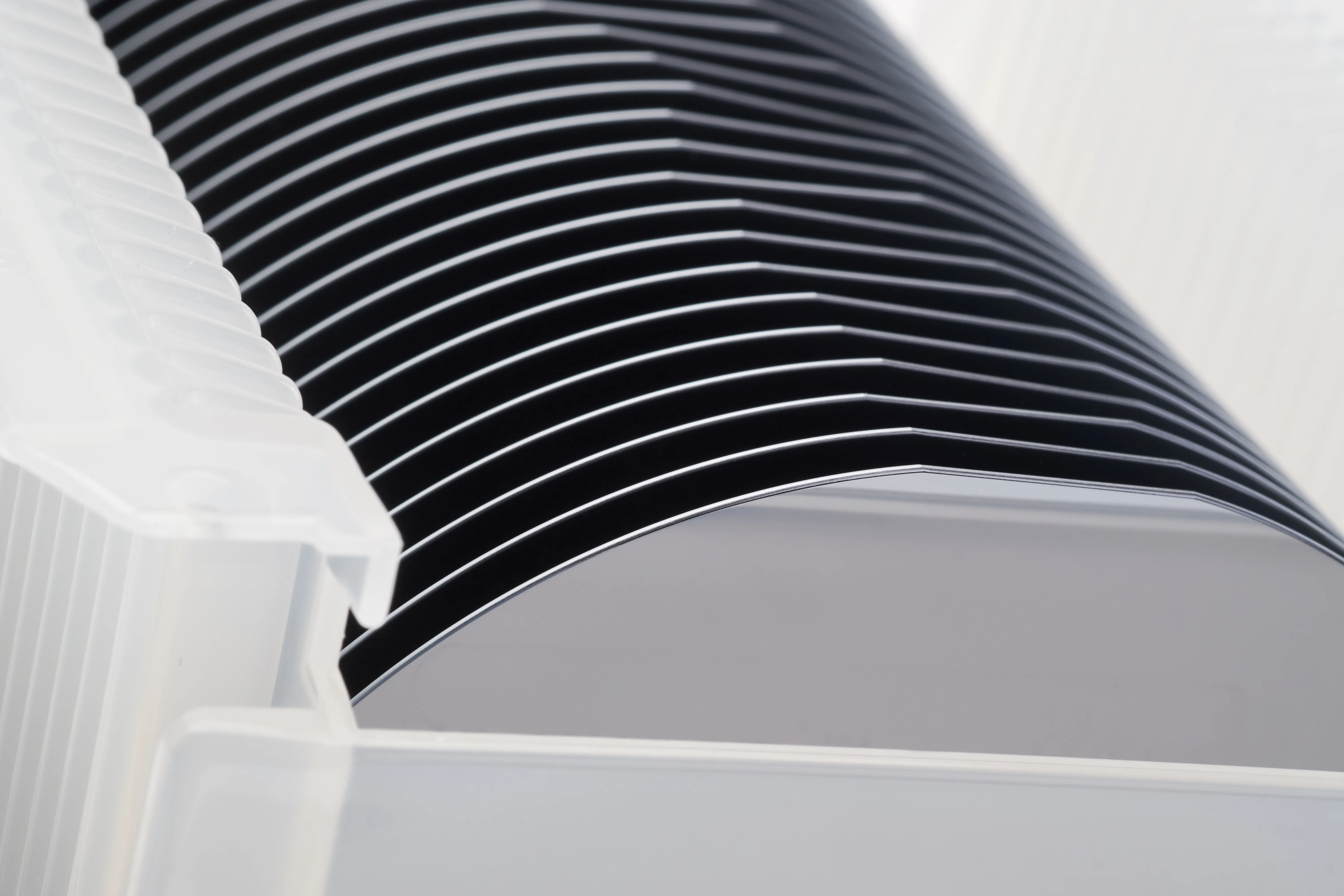
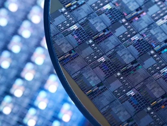
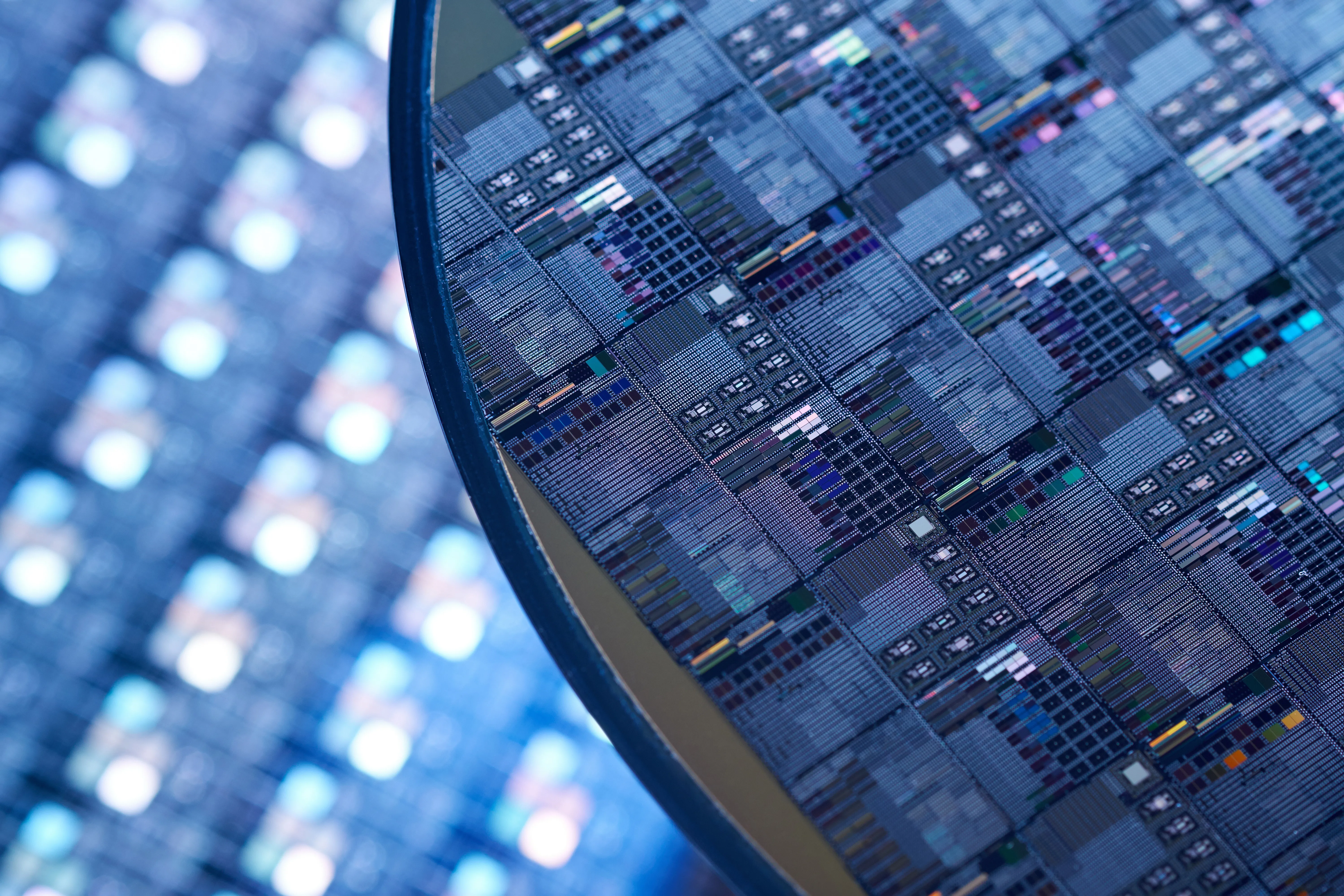
SEMI spoke with Udo Gómez, senior vice president at Robert Bosch GmbH, about MEMS technology requirements relative to standard IC design and manufacturing. Gómez highlighted solutions to challenges of MEMS technology development and manufacturing ahead of his presentation at the 22nd Fab Management Forum at SEMICON Europa 2018, 13-16, November 2018, in Munich, Germany. To register for the event, click here.SEMI: Regarding standard processes for MEMS, the situation used to be known as the MEMS law: "one product, one process." Today, the variety of MEMS sensors and their application requirements have drastically increased. What is the status of process standardization today?Gómez: Today, standardization in MEMS is certainly not as advanced as it is for conventional semiconductor processes and model environments. However, MEMS technology has developed very much in recent years. The understanding of the numerous interactions between mechanical, chemical and electrical parameters has grown enormously. Improved process tolerances and optimized simulation tools already allow the design of standard components and their manufacture using largely standardized processes and systems.This also enables standardized MEMS process platforms in foundries for fabless suppliers, since adapting process parameters to standard designs no longer means maximum effort. But the situation changes significantly if you want to implement more powerful MEMS components for demanding applications. In this case, much effort is still required in technology development to bring new and innovative designs to mass production readiness.SEMI: How does this situation interfere with the need for a fast, market-driven product development and production ramp-up?Gómez: The constant advancement of (MEMS) technology to new limits requires enormous efforts and time. Thus, fast product cycles in consumer electronics (CE) pose particular challenges. Close interaction between product and technology development is a key success factor here, as well as a deep understanding of the cause-effect relationships. This is the only way to identify and minimize process risks at an early stage.However, the steep product ramp-ups usually required in CE also offer advantages, since learning curves are run through at much shorter time-intervals than, for example, the comparatively slow ramp-ups in the automotive industry. In this way, automotive products benefit directly from the results of CE components. Conversely, CE products benefit from the higher requirements in the automotive sector, whose technologies can be developed and tested on longer time scales.SEMI: What are the critical and different design and manufacturing requirements for MEMS products versus standard IC products, which typically run in highly standardized processes?Gómez: A very special feature of MEMS devices is their multi-physics character – mechanical, electrical, magnetic, fluidic, and even chemical and/or optical effects may play a role. This is very different from standard semiconductors. Depending on the type of sensor or actuator, dedicated and often quite sophisticated models need to be developed to ensure proper function of the device – and not least to ensure full functionality after misuse. For example, shocks or drop events are usually not relevant for standard ICs but they may be extremely relevant for MEMS devices with their fragile mechanical structures.Similarly, the influence of packaging effects like bending or thermomechanical stress may be much more significant in MEMS devices than for standard semiconductors. And last but not least, a physical/magnetic/chemical/optical … stimulus usually needs to be applied when testing MEMS devices. All of this adds complexity to the manufacturing flow and requires dedicated know-how both during the engineering stage and in mass production.SEMI: BOSCH is working to extend the process platform to include complex 3D structures. What are the advantages and benefits of using 3D structures compared to standard 2D structures? Are there 3D structured products already in mass production?Gómez: We have recently extended our well-established surface micromachining process for MEMS inertial sensors (which basically uses one functional silicon layer for the movable MEMS device) to an advanced process using a second functional micromechanical layer. This opens up a large variety of design options and allows the realization of entirely new sensor topologies. For example, our most recent z-axis accelerometers for automotive and CE applications have 3D-like structures for the movable mass.This has several advantages: Firstly, the sensors can be further miniaturized as they now have fixed electrodes for capacitive readout above and below the movable mass, i.e. a larger capacitance per area. Secondly, due to their improved symmetry, these sensors have greatly improved immunity against several parasitic effects, e.g. mechanical stress from soldering or bending on a PCB. Overall, this technology enables us to offer better performance at still very competitive product size and cost. Both automotive and CE sensors are in high volume production for different applications and customers. SEMI: What do you expect from SEMICON Europa 2018 and why do you recommend attending the Fab Management Forum?Gómez: After our very positive impressions of SEMICON Europa 2017, we are convinced that SEMICON 2018 will again meet with widespread interest within the semiconductor industry. SEMICON is an excellent opportunity for us to meet our customers and partners. The Fab Management Forum, which ideally takes place parallel to SEMICON, is a highly valuable addition for us to exchange ideas with leading industry partners and to gain new insights into current trends and technical progress. Within that context, the Forum will make a valuable contribution toward strengthening the European position in semiconductor and MEMS manufacturing. As senior vice president of Robert Bosch GmbH, Dr. Gómez heads Sensor Engineering at Bosch Automotive Electronics (AE/NE-SE) in Reutlingen, Germany, the world’s largest MEMS supplier serving the Automotive, Consumer Electronics and IoT industry. Dr. Gómez started his career at Robert Bosch GmbH in 1999 at Corporate Sector Research and Advanced Engineering (MEMS technology) after completing his doctorate in physics. Before joining Bosch Automotive Electronics in April 2018, he worked in various management positions at Bosch and also held the position of Chief Expert for MEMS sensor technology. From 2013 to March 2018, he was Chief Technical Officer of Bosch Sensortec GmbH - a fully-owned subsidiary of Robert Bosch GmbH, responsible for research and development of micro-electro-mechanical sensors (MEMS) for consumer electronics, smartphones, security systems, industrial technology and logistics.Dr. Gómez has served as Deputy Chairman of the Board of VDE/VDI-Society Microelectronics, Microsystems and Precision Engineering (GMM) since 2014 has been a member of the GSA (Global Semiconductor Alliance) EMEA Leadership Council since 2015.Serena Brischetto is a marketing and communications manager at SEMI Europe.