downloadGroupGroupnoun_press release_995423_000000 copyGroupnoun_Feed_96767_000000Group 19noun_pictures_1817522_000000Member company iconResource item iconStore item iconGroup 19Group 19noun_Photo_2085192_000000 Copynoun_presentation_2096081_000000Group 19Group Copy 7noun_webinar_692730_000000Path
Skip to main content
Default Banner Image

fan-out packaging

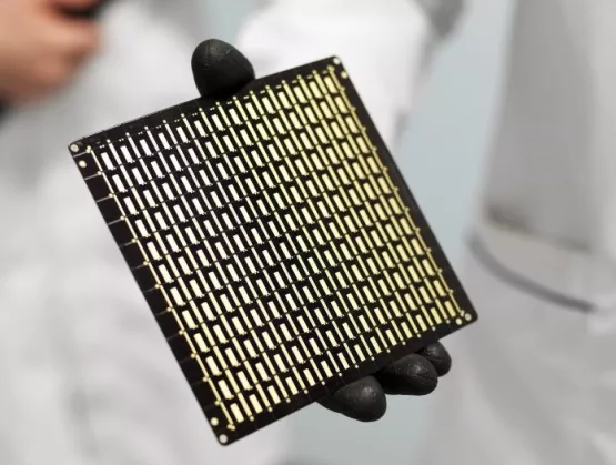
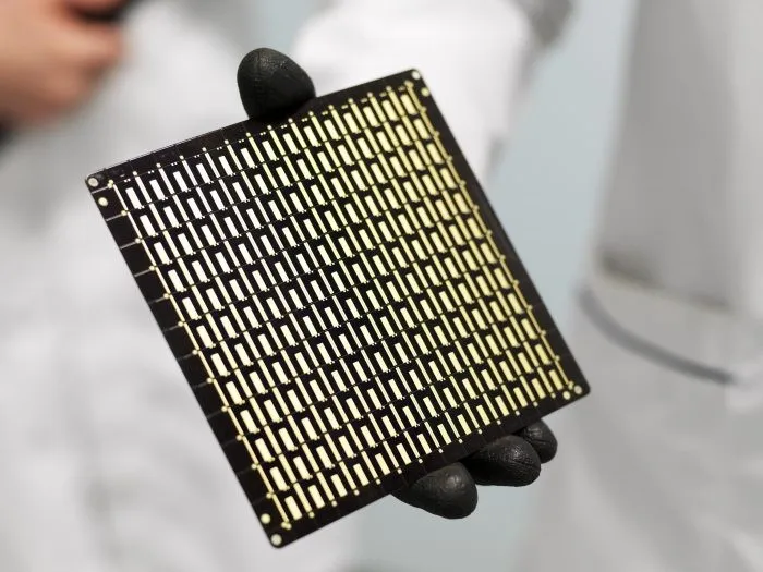
SEMI met with Martin Schrems, director of Strategy and Business Development at AT S AG, to discuss Fan-Out technology trends ahead of SEMI 3D Systems Summit in Dresden, Germany.SEMI: What are the AT S AG mission and vision and your role within the company?Schrems: AT S AG is evolving from a pure PCB manufacturer towards an interconnect solution provider. We can clearly see a continued trend towards miniaturization and modularization by (3D) integration of components such as integrated circuits and passives. Module sizes tend to increase by integrating more functions and system-level requirements. As a PCB maker, we have served such system-level requirements for a long time. Further integration offers opportunities to embed components in PCBs or substrates, offer layout and simulation services, as well as provide assembly and test services depending on specific customer requirements. As director of Strategy and Business Development, I work with my colleagues in AT S, customers, and partners across the industry towards understanding and leveraging this major transformation in the electronics industry.SEMI: What project are you currently working on that you think will make a difference in 2019?Schrems: There are number of very exciting projects, many of them already involving AT S contributions to module integration. Some of these projects involve key customers directly. We see exciting opportunities for integration of larger multi-function modules by combining PCB, substrate, and embedding core competences.SEMI: The focus of your presentation at the 3D Systems Summit will be on "Fan-Out System-in-Board technology enabling module and system-level integration.” What do you see as the key trend in this area?Schrems: Fan-Out technologies are used to distribute I/O pad connections of nanoCMOS ICs over a larger area. This relaxes bump pitch and feature size requirements for subsequent system-level PCB interconnects. In some cases, Fan-Out layers already provide a substitute to currently used Flip-Chip substrates. Well-known examples are Fan-Out packages for application processors for smartphones. There is definitely a trend in the market towards Fan-Out for high-end processor applications. Advantages of such Fan-Out packages are shorter electrical connections and a reduced thickness.However, one weakness of current Fan-Out packages is that only a limited number of components can be integrated due to mechanical stability challenges – a barrier to further component integration in larger modules. Currently, the only way to integrate more components is to use laminate-based PCBs and substrates with conventional Surface Mount Technology. Recent proposals like our “Fan-Out System-in-Board” (FO-SiBTM) technology are expected to provide an alternative Fan-Out packaging option at the board-level in the future.SEMI: Please elaborate. Schrems: Fan-Out capability and integration of more components – typically up to the 100 and more needed for electronics integration at system level – can be achieved simultaneously by combining technologies from the PCB and the packaging world. PCB laminates such as glass particles and organic materials provide mechanical stability for large boards. The recent introduction of substrate-like PCBs (mSAP) has already paved the way to cover applications that were reserved for substrates and classical packaging in the past.With FO-SiBTM technology, we have taken it a step further and offer the option to integrate SAP substrate layers onto the PCB with lines/spaces below 10µm. FO-SiBTM makes it possible to directly contact nanoCMOS chips on PCBs without any intermediate substrates. Further adding Cu pillar technology at panel level will enable Fan-Out structures even for surface-mounted components, making recent R D on panel-level Cu pillar technology very important. Through joint R D, we can drive progress in the industry to further enable cost-effective heterogeneous 3D integration.SEMI: What are your expectations for the 3D Systems Summit in Dresden, and why do you recommend your members and other industry leaders to attend?Schrems: The 3D summit is the high-level conference where key electronics industry players discuss major heterogeneous integration trends. Therefore, we very much appreciate the opportunities to exchange ideas across the supply chain including users, developers of integrated electronics hardware and tool manufacturers. Serena Brischetto is a marketing and communications manager at SEMI Europe.
Read More
SEMI met with Jay Zhang, business development director at Corning Incorporated, to discuss recent innovations at Corning that allow fine granularity CTE engineering as well as high Young’s modulus. We also talked about the impact of this work on in-process warp control, as well as the associated production methodology that provides rapid prototyping and high-volume manufacturing. We spoke ahead of his presentation at the 3D Systems Summit, 28-30 January, 2019, in Dresden, Germany. To register for the event, please click here.SEMI: What is Corning’s mission and vision and your role within the company?Zhang: Corning is one of the world’s leading innovators in materials science with a track record of 165+ years of life-changing innovations. We excel in glass science, ceramics science, and optical physics and succeed through sustained investment in RD E. Our products include Corning® Gorilla® glass, a durable material used on more than six billion mobile devices worldwide, and industry-leading LCD glass for display applications. We have recently dedicated a unit of the company called Precision Glass Solutions to address the emerging need for glass in the semiconductor industry. Here we apply Corning’s long history of glass science expertise and deep customer relationships in consumer electronics to support cutting-edge applications like wafer-level optics for precise 3D sensing and carrier solutions for temporary bonding applications in semiconductor manufacturing. It’s our most recent work in the Carrier Solutions product line that I’m excited to present: a new carrier glass product optimized for fan-out, called Corning Advanced Packaging Carriers.SEMI: What projects are you currently working on that you think will make a difference in 2019?Zhang: My team is excited to introduce Corning Advanced Packaging Carriers this year. This is a new line of product within our portfolio of Carrier Solutions. These ultra-flat glass carriers are specially developed to reduce customers’ challenge of in-process warp by up to 40 percent, which in turn helps advanced packaging customers achieve better yield.Corning Advanced Packaging Carriers feature high-stiffness properties and are available in a wide range of coefficients of thermal expansion (CTE) in fine granularity. These attributes help customers select an ideal glass carrier that will minimize in-process warp for their package. Furthermore, we make sample quantities of these carriers available in just four to six weeks to help maximize efficiency during customers’ R D process.My team is excited about the potential of this new product, but also encouraged by our results. We have already supplied this product and have heard from one of the largest semiconductor companies in Taiwan that it has reduced in-process warp by as much as 150μm.SEMI: Your presentation at the 3D Systems Summit will focus on Agile Manufacturing of Glass Carriers for Advanced Packaging. What exactly will you be sharing?Zhang: There is a lot of interest right now in using glass as a carrier substrate in temporary bonding applications in advanced semiconductor packaging – especially in fan-out processes. We also know that in-process warp is a significant challenge to companies pursuing advanced packaging because different CTE materials are added during the process. My team has done a lot of work to understand the impact that an ideal CTE glass carrier substrate can have on minimizing in-process warp. We have studied the available levers – both theoretical and in real-life fab environments – that can help address this challenge. I will present our findings on how it is possible to select a glass carrier with the ideal CTE and Young’s modulus to reduce in-process warp by up to 40 percent, and how Corning has developed an agile manufacturing platform to support customers with these ideal carriers from their R D stage through mass production.SEMI: What do you think will be a hot topic in the next few years?Zhang: We expect high-end fanout technology to address more applications beyond just mobile APs. There is also an interesting dynamic playing out between wafer-level and panel-level fan-out technologies. Corning is active in both areas. In developing and offering high performance glass carriers, we hope to help enable our customers to expand the fan-out applications space.SEMI: What are your expectations regarding the summit in Dresden, and why do you recommend your members and other industry leaders to attend the 2019 3D Systems Summit?Zhang: Europe is where some of the most advanced packaging technologies are born. Fan-out also saw early commercialization there. I hope to meet many scientists and technologists at 3D Systems Summit and exchange technical and business ideas. We also hope to get early feedback from other attendees about the value of our new product offering. Serena Brischetto is a marketing and communications manager at SEMI Europe.
Read More