downloadGroupGroupnoun_press release_995423_000000 copyGroupnoun_Feed_96767_000000Group 19noun_pictures_1817522_000000Member company iconResource item iconStore item iconGroup 19Group 19noun_Photo_2085192_000000 Copynoun_presentation_2096081_000000Group 19Group Copy 7noun_webinar_692730_000000Path
Skip to main content
Default Banner Image

3D Heterogeneous Integration

SEMI met with Martin Schrems, director of Strategy and Business Development at AT S AG, to discuss Fan-Out technology trends ahead of SEMI 3D Systems Summit in Dresden, Germany.SEMI: What are the AT S AG mission and vision and your role within the company?Schrems: AT S AG is evolving from a pure PCB manufacturer towards an interconnect solution provider. We can clearly see a continued trend towards miniaturization and modularization by (3D) integration of components such as integrated circuits and passives. Module sizes tend to increase by integrating more functions and system-level requirements. As a PCB maker, we have served such system-level requirements for a long time. Further integration offers opportunities to embed components in PCBs or substrates, offer layout and simulation services, as well as provide assembly and test services depending on specific customer requirements. As director of Strategy and Business Development, I work with my colleagues in AT S, customers, and partners across the industry towards understanding and leveraging this major transformation in the electronics industry.SEMI: What project are you currently working on that you think will make a difference in 2019?Schrems: There are number of very exciting projects, many of them already involving AT S contributions to module integration. Some of these projects involve key customers directly. We see exciting opportunities for integration of larger multi-function modules by combining PCB, substrate, and embedding core competences.SEMI: The focus of your presentation at the 3D Systems Summit will be on "Fan-Out System-in-Board technology enabling module and system-level integration.” What do you see as the key trend in this area?Schrems: Fan-Out technologies are used to distribute I/O pad connections of nanoCMOS ICs over a larger area. This relaxes bump pitch and feature size requirements for subsequent system-level PCB interconnects. In some cases, Fan-Out layers already provide a substitute to currently used Flip-Chip substrates. Well-known examples are Fan-Out packages for application processors for smartphones. There is definitely a trend in the market towards Fan-Out for high-end processor applications. Advantages of such Fan-Out packages are shorter electrical connections and a reduced thickness.However, one weakness of current Fan-Out packages is that only a limited number of components can be integrated due to mechanical stability challenges – a barrier to further component integration in larger modules. Currently, the only way to integrate more components is to use laminate-based PCBs and substrates with conventional Surface Mount Technology. Recent proposals like our “Fan-Out System-in-Board” (FO-SiBTM) technology are expected to provide an alternative Fan-Out packaging option at the board-level in the future.SEMI: Please elaborate. Schrems: Fan-Out capability and integration of more components – typically up to the 100 and more needed for electronics integration at system level – can be achieved simultaneously by combining technologies from the PCB and the packaging world. PCB laminates such as glass particles and organic materials provide mechanical stability for large boards. The recent introduction of substrate-like PCBs (mSAP) has already paved the way to cover applications that were reserved for substrates and classical packaging in the past.With FO-SiBTM technology, we have taken it a step further and offer the option to integrate SAP substrate layers onto the PCB with lines/spaces below 10µm. FO-SiBTM makes it possible to directly contact nanoCMOS chips on PCBs without any intermediate substrates. Further adding Cu pillar technology at panel level will enable Fan-Out structures even for surface-mounted components, making recent R D on panel-level Cu pillar technology very important. Through joint R D, we can drive progress in the industry to further enable cost-effective heterogeneous 3D integration.SEMI: What are your expectations for the 3D Systems Summit in Dresden, and why do you recommend your members and other industry leaders to attend?Schrems: The 3D summit is the high-level conference where key electronics industry players discuss major heterogeneous integration trends. Therefore, we very much appreciate the opportunities to exchange ideas across the supply chain including users, developers of integrated electronics hardware and tool manufacturers. Serena Brischetto is a marketing and communications manager at SEMI Europe.
Read More
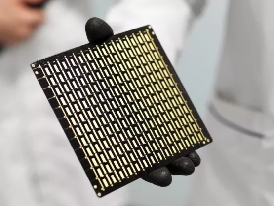
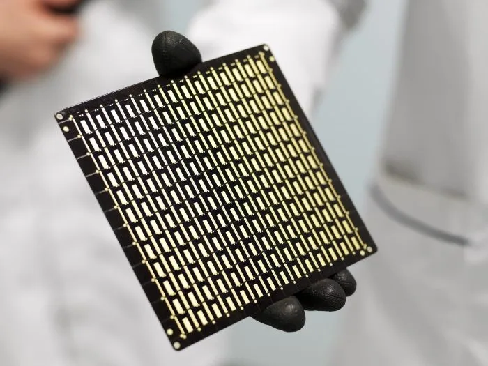
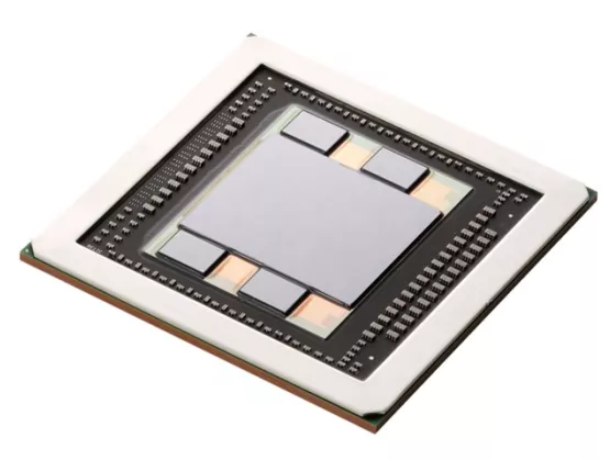
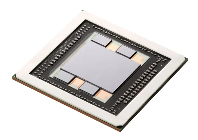
SEMI met with Gerald Beyer, program manager at imec, to discuss the co-existence of various 3D interconnect technologies and their need for new materials and integration solutions. The two talked in the runup to his presentation at the Advanced Packaging Conference at SEMICON Europa 2018, 13-16, November 2018, in Munich, Germany. To register for the event, click here. SEMI: Can you confirm this trend towards heterogeneous integration and do you think it will be a long-term development trend?Beyer: We consider heterogeneous integration as a scaling booster for functional partitioning and as a fashion method to create systems, which would not be possible or economical on such as a single chip. As you can apply it to numerous systems, we expect it to stay for the long term.SEMI: What are the new critical challenges for the combination of different technologies into one package?Beyer: When you create a complex system, there is usually more than just one challenge. On one side, you need to be able to design such a system. If you disintegrate a large chip, you need to decide how to reconstruct it, i.e. which function goes into which strata. You would like to do that not manually but with a set of tools supporting the designer. Only recently EDA (Electronic Design Automation) and design houses have started to support this idea.On the technology side, interconnections between some strata of such a reconstructed chip will require small pitch interconnects of the order of 1µm pitch and less. Today, wafer-to-wafer bonding technologies have sufficient overlay margins for 1µm pitch. Wafer-to-wafer bonding technologies, however, have a number of constraints such as equal die size and the necessity to realize chip stacking rather in a fab environment than in a traditional packaging house. Die-to-wafer assembly technologies still need to bridge the gap to deep sub 10µm pitch in terms of alignment and cleanliness.SEMI: What kind of new materials or integration solutions do you expect to be developed? Are you working on it already?Beyer: As explained above, die partitioning requires sub 1µm pitch interconnects. We are investigating fine pitch wafer-to-wafer and die-to-wafer (direct) bonding. For the latter, not only new alignment capabilities but also die cleaning and thin die handling technologies need to be developed. To build a complete system with data processing, memories etc., novel integration schemes such as Flip Chip – Fan Out Wafer Level Packaging with high density 2D and 3D interconnect capabilities are being investigated. These new systems differentiate from current ones by high density Through Package Vias (TPV), Si bridges and sub 2µm line/spacing RDL. The new integration approaches push the materials such Temporary Bond Materials (TBM), Wafer Level UnderFill’s (WLUF), photo patternable polymers for fine Line/Spacings to name a few, to the limits. Hence, development of new materials is a key aspect.SEMI: What trends and developments do you expect in the near future and why would you recommend attending the Advanced Packaging Conference?Beyer: The development and commercialization of products using heterogeneous integration is a big effort drawing on resources from EDA vendors, materials and packaging tool suppliers, OSATs, foundries, memory suppliers and IEDMs and academia alike. The agenda of the Advanced Packaging Conference at SEMICON Europa reflects this diversity and I am looking forward to interesting discussions with all participants. Gerald Beyer has been working in the field of 3D Technologies since 2012 as the technology program manager of the 3D System Integration Program of imec. Prior to this role, he was the interconnect program manager and group leader of BEOL integration. He received a PhD in materials science from Imperial College, London and a MSc from Thames Polytechnic, London.Serena Brischetto is a marketing and communications manager at SEMI Europe.
Read More