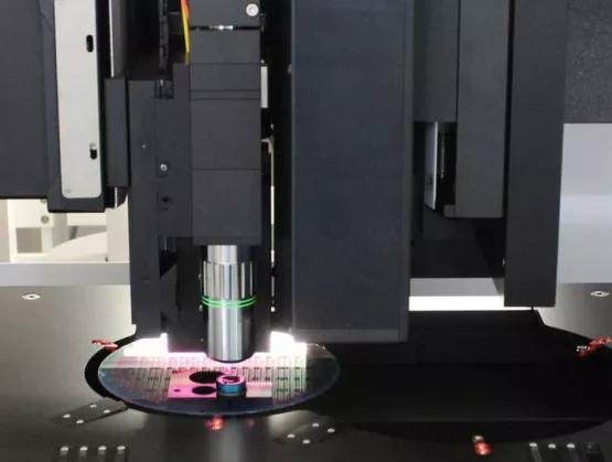
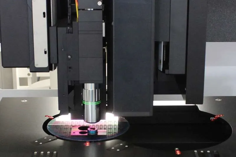
Semiconductor fabs have been getting smarter and smarter over the past 30 years. It’s a natural evolution – the direct outcome of numerous continuous-improvement efforts. The really important difference on the road to smarter fabs, the one change that’s enabling the Industry 4.0 revolution, is the concept of a cyber-physical system or digital twin. If you don’t have a thorough, detailed, high-fidelity digital twin of your entire fab operation, then you cannot have “Smart Manufacturing.” That’s really the definition of a smart site. A digital twin is simply a requirement for all smart factories of the future.
One caveat: No matter what you build today from a smart perspective, your digital twin’s fidelity will improve over the next 20 years.
A factory’s digital twin has two facets: the operational aspect and the yield aspect. Each of these two facets places different requirements on a database including the types of data, the frequency of data generated, the retention of data, and even the AI/ML techniques used to analyze the data. A combination of these data requirements are needed to create a digital twin – the virtual representation of your entire factory operation, whether it’s on the wafer-fab front end or the assembly and test back end.
What’s most important here is that facility-wide data sets and databases must be able to communicate with each other using refined summary statistics to create a practical digital twin. For example, a lot of information is collected on the yield side to feed the deep-learning models needed to manage processes. However, the factory scheduler, driven largely by the smart operational database, needs only summary statistics from the yield database to be able to act in the next moment or over the next 24 hours. Figure 1 illustrates the needs of and the interaction between a smart operational and a yield database.
Figure 1: The Operational and Yield databases in a Smart Factory need to exchange summary statistics.
Today, we find that although these databases generally speak to each other in smart factories, they’re still not sufficiently connected to permit the use and analysis of data needed to realize the full potential of a smart factory. That level of interconnectedness is still in the future.
Some solution providers have created what is essentially a “smart learning warehouse” (“database” has become too limited a term here). This warehouse collects, analyzes and learns from the extensive amount of information that a fab generates. Game-changing, more holistic applications become possible when this information can be combined in new and informative ways.
As it turns out, a data source is just a data source, but users in different factory areas need to extract different information from these common data sources. They need different applications and portals – in other words “views” – that are adapted and adjusted for each area’s needs.
Aren’t we smart enough?
Some people think that 300mm fabs are already smart. That’s true. They are. But, they could be a lot smarter. No 300mm fab in use today has attained the full, utopian vision of what a smart factory can deliver over the next 10 years. When you finally integrate all of the disparate databases in a fab – when you’re able to use all of those different data sources as one common data source – that’s when your Smart Factory will have the ability to self-optimize its future actions and react quickly to real-time events.
The largest semiconductor manufacturers tend to develop these smart factory applications on their own. The remaining semiconductor fabs need to work together with other fabs and their solution providers to develop these smart factory applications.
Why now?
Why is everyone talking about “Smart” now? It’s because the semiconductor industry has helped to create all of the enabling technology: the compute power, the networking and networking standards, and even the industry’s maturation into a multi-tiered organization of solution providers. We’ve reached the point where we can collect data from a widespread sensor network along with tool-health data and we can then warehouse this data so that it can be applied to more intelligent decision-making.
While there may be one or two sensors on a tool today, in the future there will be many such sensors connected over an IoT network or networks that provide mountains of data to the warehouse. All of this data will feed into the digital-twin version of the fab.
One of the biggest changes on the horizon made possible by all of this accessible data is advanced scheduling. Despite all of the automation advancements made over the past 25 years, including robotic handling, it’s still hard to decide “where, what, and when?” for every single lot in the factory. Today, no factory in the world is more complex than a semiconductor fab. Optimizing a semiconductor manufacturing process is the most complex manufacturing-optimization task in the world.
Do it for ROI
ROI is the chief reason for having a digital twin. Once you can make a truly smart, holistic schedule of the fabs operations — not a dispatch or rule-based dispatch list — then you can create an operationally smart factory. Rule-based dispatching systems primarily focus on tools and tool-centric views. Although they incorporate knowledge from current WIP and tool conditions to make decisions better than simple dispatch systems, smart factories are not just about tools and the current WIP at them. Smart factories use the status of every tool and lot in the factory to make fab-centric optimizations instead of tool-specific optimizations.
Once you have a digital twin, you’re optimizing for global functions such as line linearity and on-time delivery. These functions are not just about the moment. The transition to a smart factory thus represents a huge philosophical change.
When you know exactly what’s going to happen in a factory over the next 12 hours for every single lot, every single wafer carrier, and every single entrance port of every tool in the factory, then you suddenly have control over the factory’s idle time. You know when you can optimally perform PM (preventive maintenance). You know how to best redirect material or labor resources to maximize output. You can create a smart schedule for every maintenance person in the factory that comprehends each person’s skill set and tool downtime so that there’s no negative impact on the factory’s productivity. You can only do all of this when you know the future.
Figure 2 illustrates the opportunity. Imagine that a factory contains 1,500 tools. Use of these tools is scheduled for the next twelve hours. The information depicted in Figure 2 encompasses process changes from one chemistry to another, implant changes, reticle changes, and the status of every single consumable for all 1,500 tools. The white spaces that appear between processes in Figure 2 represent opportunities to intelligently schedule events such as maintenance to maximize factory productivity.
Figure 2: Smart scheduling permits factory-wide optimization to maximize productivity.
Once you have a schedule, you need to translate that schedule into actions or movement. It’s not easy to do this and most material-control systems today make overly simplistic decisions based on modeled assumptions and typical cases rather than the actual time each lot needs to be at a precise location, which can only come from a schedule. Once the data from all of the tools is connected, a smart scheduling system can use the digital twin to make far better process decisions. The larger the factory (or more complex the factory), the more important it is to make smarter decisions.
Note: SEMI has a Smart Manufacturing Technology Community. For more information or to get involved, click here.
If you would like to discuss Smart Manufacturing more with John directly, he can be contacted at [email protected].
John Behnke is general manager of the Final Phase Systems product line at INFICON.