downloadGroupGroupnoun_press release_995423_000000 copyGroupnoun_Feed_96767_000000Group 19noun_pictures_1817522_000000Member company iconResource item iconStore item iconGroup 19Group 19noun_Photo_2085192_000000 Copynoun_presentation_2096081_000000Group 19Group Copy 7noun_webinar_692730_000000Path
Skip to main content
Default Banner Image

defect detection

Traditionally, defect classification is done manually by operators or using Automated Optical Inspection (AOI) machines, often leading to classification inconsistencies. Also, rules-based AOIs may at times be unable to fully satisfy project requirements due to the rigidity of inspection recipes. 
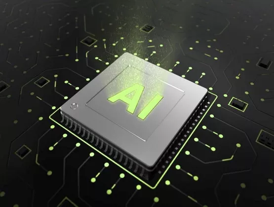
SixSense – Breaking the Status Quo with Artificial Intelligence Enter SixSense, an AI-powered defect classification software platform that has been making breakthroughs in defect detection and classification for semiconductors to make manufacturing smarter and more efficient. Founded in 2018, SixSense has already amassed a wealth of experience and chalked up a number of successes such as automating the manual image classification process, reducing manufacturing false rejects, and capturing escapees. Infineon Technologies and GlobalFoundries were amongst the early adopters of SixSense’s platform: classifAI. With Infineon, classifAI has allowed over-rejection rates to be precisely quantified. classifAI – Simple UI, Easy Usage, Powerful Models As a UI-based assistive software platform, classifAI, SixSense’s automated defect classification platform is built with the defect and yield engineer in mind. SixSense takes care of all the back-end complexities – such as coding, algorithm modelling and deployment – to enable end users to get started and use the platform with a simple GUI. The simplified end-to-end AI pipeline offered on the platform includes data labelling to make data AI-ready, model training, and model testing. Ultimately, models are deployed on the production floor for 24/7 inferencing of hundreds of millions of images every year, at scale, across processes, tools and sites. Machine learning models built by the SixSense team have seen strong results, with model accuracy of up to 98% in certain use cases. Track Record of delighting IDMs, Foundries and OSAT Customers SixSense has consistently solved visual inspection problems and enabled the success of IDMs, foundries and OSATs since its inception. The AI technology has helped a range of customers across 100mm-300mm wafer standards, both pure silicon and compound wafers, and caters to specific end-use market requirements such as RF and automotive. Partnerships between startups and established manufacturers are key to actualizing the value of AI in manufacturing. “Our collaboration with AI startup SixSense has enabled us to explore opportunities in yield gain, improving cycle time, and real-time monitoring of process shifts,” said Dato’ Tan Soo Hee, Executive Vice President, Global Backend Operations at Infineon Technologies Asia Pacific. “SixSense has been very attentive to the needs of our engineering team, addressing project requirements using a customer-first approach evident in the design of the intuitive software platform,” said Melvyn Peh, Principal Engineer, Automation-Scan-Pack, Infineon Technologies Asia Pacific. The intelligent annotation module is one of many offered by SixSense, which uses AI to train AI and accelerate the data annotation process by focusing on the semiconductor-specific requirements. 
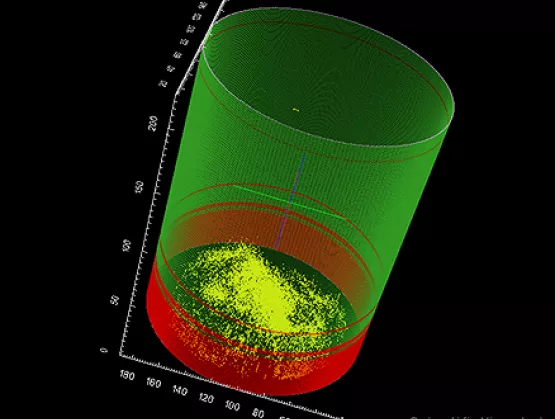
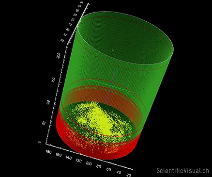
Another valuable module in classifAI is advanced analytics that capture the heatmap for defect distribution on the images. Images are stacked on top of each other, with the location of defects aggregated to provide the defect heatmap. Through this, systematic failure patterns were identified that allowed defect engineers to zero in on key sources of failure and assist in root-cause analysis. Infrastructure – Scale Fast, Adapt Quickly, Accelerate Value Creation In the dynamic world of technology, machine learning and AI projects must meet changing infrastructure demands. A cloud-first approach is often favored for the plethora of benefits it offers. “We’re looking forward to a great partnership with SixSense, treading together hand in hand exploring fresh ideas and possibilities,” said Manju Jalali, Vice President of digital manufacturing at GlobalFoundries, who oversees the company-wide roll out of classifAI. For use cases where on-premise deployments are preferred, SixSense offers such options for infrastructure integration, satisfying all possible infrastructure requirements in the market. Contributing to a vibrant innovation ecosystem SixSense was mentioned by Singapore’s Deputy Prime Minister Heng Swee Keat during an event that marked Infineon’s 50th anniversary in Singapore: “I am heartened that Infineon will be investing more than $27 million over three years on an AI initiative in Singapore. Under this initiative, Infineon Singapore will be partnering academia, industry, and local startup SixSense AI to develop new AI solutions and courses.” Explosive Growth of AI in Chip Manufacturing According to a McKinsey Company report, AI contribution to semiconductor company earnings is projected to rise to between $85 billion and $95 billion per year in the coming years. SixSense has been taking great strides in creating value for their semiconductor customers. “SixSense offers tremendous value in a high-growth vertical in the semiconductor industry, marrying the latest deep learning algorithm with the compute power of the cloud,” said Rajan Rajgopal, CEO of DenseLight Semiconductor. “This leads to faster root-cause analysis that helps reduce the cost of non-conformance and improve quality.” Dominic Teo is Enterprise Business Development Representative at SixSense. He can be reached at [email protected].
Read More
Sapphire is a precious gemstone, consisting of aluminum oxide (α-Al2O3) with occasional traces of other elements such as iron, titanium, chromium, vanadium or magnesium. While sapphire stones found in nature mostly go to jewelry applications, the lab-grown sapphire – produced in a scale of up to several hundred tons per year – is widely used by the electronic industry. Now one can hardly find a branch of technology where this crystal is not used.Sapphires are mainly applied in infrared optical components, high-durability windows, wristwatch crystals, and the very thin electronic wafers used as the insulating substrates of solid-state electronics. High thermal conductivity, low reactivity, and appropriate unit cell size make sapphire an ideal material for a wide range of such electronic substrates for manufacturing of components such as LEDs and CMOS chips.SEMI spoke with Ivan Orlov, CEO of Scientific Visual, after his presentation at SEMI Strategic Materials Conference at SEMICON Europa, 12-15 November, 2019 in Munich, Germany, to learn more about the future of sapphire.SEMI: Why is sapphire an ideal material for a wide range of electronic substrates? Orlov: Sapphire undoubted advantages are its chemical inertness and ability to withstand high temperature, radiation and mechanical loads. In addition, it exhibits low dielectric loss and very good electrical insulation that makes sapphire a good candidate for substrates for LEDs and laser diodes or wafers for epitaxial growth. However, the most important advantage is that sapphire crystal lattice does very well matching semiconductor materials deposited to its surface, in particular nitrides of group III elements. To plainly benefit from these features, the grown sapphire must have as few macro- and micro-defects as possible, as substrate defects are inherited by semiconductors layers grown on the substrate surface. Hence the importance to detect defects in the raw sapphire material. This is the area where our team at Scientific Visual contributes. SEMI: Flaws are usually identified only after costly wafering and polishing steps, because rough surface of raw crystals prevents detection of the defects. What can be done to prevent defects?Orlov: Today, major players are investing in growing larger crystals without mastering in depth the growth process. Let’s face it, the semiconductor substrate industry, which is primarily based in Asia, is using empirical research methods. The raw sapphire boules are still inspected manually, and this qualitative assessment is exploited in two folds. The first step is to further process the boule. Furnace operators then adjust the growing parameters depending on the results of the manual inspection.Due to the lack of visibility into internal crystal defects, the crystal growth and its downstream processing remain an art rather than a science. The primary reasons are the difficulty to measure, locate and quantify precisely the defects in the full crystal volume. Scientific Visual equipment enables defects in raw boules to be fully quantified and categorized. With such objective measurements and knowing the full set of growth parameters, the Process Engineering (PE) team can, with the assistance of deep learning algorithms, considerably improve the growing process. Our quality control tools give Process Engineering team the “eyes” to see complete defect distribution in raw crystals, enabling it to make minor modifications in the growth process to improve yields, reduce costs and shorten the time to market for products.SEMI: What lead to those advancements and what problems did your team set out to solve? Orlov: Breakthroughs in immersion tomography, machine vision and parallel computing drove advancements in automated quality control technology. Previously crystal inspection accuracy was limited by the acuity of the operator’s eye and subjective bias. Light distortion and the diffusion of crystals made it impossible to accurately identify internal defects.Scientific Visual equipment give operators an undistorted 3D view of all defects in a crystal boule or ingot. However, only deep learning technology can correlate a hundred thousand growth data points to identify a final defect pattern.Defect pattern in non-processed item cored from EFG sapphire plate. Well visible is a typical wavy pattern of surface layers and sandwich structure in the volume. Color code marks sapphire defect density: from deep blue (non-defective material) to deep red (highest defectiveness.) SEMI: What challenges are addressed by your approach? Orlov: Increasing the yield of semiconductor substrates like Sapphire, Gallium Nitride and Silicon Carbide is paramount to reducing the price of wafers while increasing their quality. The upstream growth and downstream wafering processes are not deterministic. So far, most of the producers can only determine the quality during the late stages of the process. This condition creates huge constraints for teams in charge of production and processing. Automated Quality Control (QC) at the early stage of the production chain relieves all the unknowns, ultimately reduce the cost of material.SEMI: And what are the main opportunities?Orlov: There are massive opportunities to increase the yield and to ease the full processing chain from growth to the wafering process. Objective Quality Control (OQC) paves the way to industry-wide standards that categorize crystal quality at each step of growth to enable full certification of the defectiveness of the material and facilitate its trade and exchange.SEMI: What’s one of your predictions for the future of new materials?Orlov: The explosion of e-mobility and electric vehicles and the development of other green technologies will drive rising demand for low-defect sapphire, silicon carbide and gallium nitride substrates thanks to the streamlining of the full processing chain. Manual quality control will soon give way to full automation as quality control in sapphire and other raw crystals production is the only missing link in a fully automated semiconductor production chain. I believe that in five years, automated raw crystal inspection will become standard in the industry. Our mission is to empower every crystal grower to achieve this important milestone.Dr. Ivan Orlov obtained a Ph.D. in Crystallography from the Federal University of Technology in Switzerland EPFL and an MSc in Solid-State Physics in Moscow, Russia. Ivan co-founded Scientific Visual in 2010 to answer the challenge of the synthetic crystals industry struggling with high defect yield. Prior to this he worked in a company specialized in diamond optics. He has more than 10 years of experience in R D with focus on optical materials, industrial crystals and non-destructive quality control technologies. Dr. Orlov was a SEMI Task Force member for sapphire standard development in China and collaborates with ISO committee in Switzerland to establish industry-wide sapphire quality standards.Serena Brischetto is senior marketing and communications manager at SEMI Europe.
Read More