downloadGroupGroupnoun_press release_995423_000000 copyGroupnoun_Feed_96767_000000Group 19noun_pictures_1817522_000000Member company iconResource item iconStore item iconGroup 19Group 19noun_Photo_2085192_000000 Copynoun_presentation_2096081_000000Group 19Group Copy 7noun_webinar_692730_000000Path
Skip to main content
Default Banner Image

materials science

Materials science – a field that includes elements of applied physics, chemistry, and mulit-disciplinary engineering applied to magnetics, metallurgy, ceramics, polymers and silicon – serves as the foundation for technologies that have driven much of the tech sector’s economic growth for the past 50 years. As our devices grow smaller, faster and smarter – while also requiring higher performance and greater energy efficiency – we’re reaching the limits of what can be accomplished with these fundamentals. The technology sector needs renewed research and investment in new materials to help address the challenges we face in a rapidly changing world. Leading TDK Ventures, the investment arm of TDK Corporation, I’m happy to report that a number of young companies have stepped up to the challenge of innovating materials science for the 21st century. In the past 18 months, we invested in multiple startups dedicated to reimagining the basic building blocks of materials science and identifying new ways to push technology forward – in fact, three of them have successfully gone public or been acquired over the last year. This demonstrates not just a renewed interest in materials science research but also highlights the momentum for healthy returns on materials science investments. Or, as I like to say, it’s the return of materials science returns. Materials science at the atom level For high-tech investors, materials science went out of favor the past 10 or 15 years, because investment in software development companies began to deliver very healthy returns in relatively short time frames – often in as little as two or three years. Product development in materials science traditionally requires much more capital and takes a lot longer to generate returns than software startups. Today’s hardware innovators are making it clear that we’ve only begun to scratch the surface of what’s possible in the materials sciences. Unlike 20 years ago, we can develop products like graphene, which consists of a single layer of carbon atoms that is about 200 times stronger than steel and an excellent conductor of both heat and electricity. Nanometer-scale materials like this enable the design of ultra-low power, high-performance components that can integrate multiple functionalities onto very small devices and create opportunities that were impossible only a few years ago. With advances like this, the future of materials science is regaining its luster. Investors welcome materials science startups Three materials science startups with successful exits: GenCell, which went public in 2020, develops fuel cell solutions that offer clean backup power for a variety of commercial, industrial and healthcare operations and can be used for off-grid power and rural electrification in a wide range of temperature and humidity conditions. GenCell’s revolutionary process creates hydrogen-on-demand from anhydrous ammonia (NH3) at 10 times the efficiency of other solutions, without any outside electrical power.GenCell fuel cells enable hydrogen and oxygen to react in an emissions-free chemical process that produces electricity and heat, with pure water as the only by-product. Origin, acquired by Stratasys in 2020, creates 3D printer platforms that offer an additive manufacturing approach to mass manufacturing, with the freedom of open materials. Using Origin 3D printers, customers can print products of their own design from a range of materials, or from their own proprietary materials. Origin maintains strategic partnerships with the largest materials science companies in the world and print products for leading companies in the dental, medical, and industrial sectors. SLD Laser, acquired by KYOCERA in 2020, produced the world's first high-luminance, fully integrated white laser light emitter. The emitter is based on a gallium nitride solid-state laser projected through a high-performance phosphor element that converts the blue laser to broad-spectrum, incoherent white light that eliminates eye safety risks. The resulting light source emits 100x more luminance, projects 10 times the distance than an LED, and is being incorporated into a range of specialty, display and automotive lighting applications. Materials matter Many of the fundamental technological innovations of the last century, including advances in semiconductors, biotechnology, and server technology, were based on breakthroughs in materials science. At TDK Ventures, we believe the only way to advance further is to return to materials research to identify new ways to expand the horizons of science and technology. For some established companies, this may require a pivot from traditional ways of getting things done and embracing fresh ways of thinking. It means thinking more like a startup and welcoming the challenges of change and new opportunities. We also believe that these innovations should not just push the boundaries of existing disciplines but contribute to preserving our environment and improving the lives of people. This is one of the founding principles of TDK Ventures: Our investments must contribute to digital and energy transformation and help lead to a more sustainable world. Our goal is to help every startup we invest in achieve their full potential for positive world impact. For instance, GenCell fuel cells bring emissions-free electrical power to rural communities far from traditional electrical grids, helping raise living standards without reliance on polluting diesel generators. Laser lights from SLD Laser are more power-efficient than traditional LED lamps, as lights last over 10,000 hours longer than equivalent HID (high-density discharge) lamps. Origin 3D printer platforms enable safe, localized manufacturing, and are geared toward minimizing energy waste in the supply chain. We’re just scratching the surface of what’s possible with materials science. At TDK Ventures, we’re dedicated to delivering meaningful financial results while exploring the potential of new and transformative technologies to bring positive change to our society and environment. Nicolas Sauvage is managing director at TDK Ventures, the corporate venture capital (CVC) arm of Japan-headquartered electronics manufacturer TDK Corporation. TDK Ventures is a technology-focused venture fund, investing globally in early-stage startups that leverage fundamental materials science to bolster innovations in Digital Transformation (DX), Energy Environmental Transformation (EX), unlocking an attractive and sustainable future for the world.
Read More
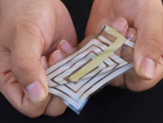
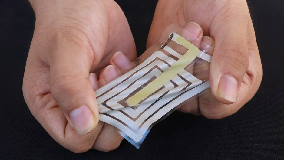
As the body’s largest organ, skin is responsible for the transduction of a vast amount of information. This conformable, stretchable, self-healable and biodegradable material simultaneously collects signals from external stimuli, which translates into information such as pressure, pain and temperature. The development of electronic materials, inspired by the complexity of this organ, offers a tremendous unrealized materials’ challenge. Fortunately, the advent of organic-based electronic materials may offer a solution to this longstanding problem.Zhenan Bao, K.K. Lee Professor of Chemical Engineering, Stanford University, is one of the world’s leading researchers working on the design of organic electronic materials that mimic skin functions. SEMI’s Maria Vetrano interviewed professor Bao to preview her February 25 keynote, Skin-Inspired Electronics, at FLEX|MEMS Sensors Technical Congress (MSTC) 2020, February 24-27, 2020, at the DoubleTree by Hilton in San Jose, California.Join us at FLEX|MSTC to meet Professor Bao and other industry influencers furthering innovation in flexible hybrid electronics (FHE) and MEMS sensors. Register now to connect with her at FLEX|MSTC or visit her on LinkedIn.SEMI: Your pioneering work on the use of electronic materials to construct second skin is a major step forward in human-machine interfaces. Could you please describe second skin?Bao: Second skin is a new electronic-device platform encompassing electronic devices that have skin-like properties such as stretchability, self‐healing ability, biocompatibility and biodegradability. In essence, the second skin is an electronic system of fully integrated multifunctional components operating on the surface of or inside the body to enable smart healthcare for disease prevention and treatment and to enhance the functional capabilities of natural skin. The second skin could also serve as a module to connect our human body to the Internet, thereby allowing human integration with the Internet of Things (IoT) for next‐generation wireless communications. In this way, we can view the second skin as an artificial body part that can be used to improve our everyday lives.SEMI: How might second skin operate in the human body?Bao: It has many potential uses. It could be a prosthesis for people who have lost their sense of touch. It could be used to repair damaged skin as well as to provide enhanced functionality that’s not possible with biological human skin. It could, for example, connect us with our external environment, with other people, even with our cars.I can also envision second skin as an implantable device for both neurostimulation and for early detection of disease. Schematic illustration of structure of second skin composed of functional devices: sensor, integrated circuit, display and power supply. Source: Stanford University SEMI: How did you get started in this research? Bao: Sixteen years ago when I started at Stanford, I learned of a colleague in mechanical engineering who was working on robotic cockroaches. That’s when I understood the need for sensor functions in robotics.I considered the large number of people with prosthetics who do not have a sense of touch. With this audience in mind, I started by designing a simple flexible electronic device that could take the shape of skin, even conforming to a robot hand, thereby approximating the natural sense of human touch.Once we developed the first sensor, and realized that its touch sensitivity could eclipse that of human touch, I asked myself: what can we learn from second skin – in addition to its sensing functionality?Skin is not just flexible; it is biodegradable and stretchable. So we started to dream. We began by developing electronic materials, either conductors or semiconductors. We added new functionality, such as self-healing properties, biodegradability and stretchability. That opened the way to new materials’ development.SEMI: What discoveries have you made in new materials?Bao: Over the past decade, we’ve developed skin-like materials with electronic properties that are on par with the best conducting and semiconducting polymers. Some of our skin-like semiconducting polymers can perform even better than amorphous silicon. That means with suitable processing methods, we can make stretchable ICs, initially with tens of transistors that can perform analog or digital functions, and in a later stage, stretchable displays driven by active matrix arrays.SEMI: What would it take to put these materials into production?Bao: We need to develop methods to pattern the skin-like electronic materials into fine features. We have been leveraging similar processes used for flexible circuit boards. Some research groups are developing roll-to-roll fabrication and printing methods.SEMI: Which technologies/applications are you commercializing?Bao: C3Nano is a Bao Research Group spin-off startup that is commercializing nanomaterials that are promising for bendable and foldable electronics.Another spin-off that is licensing our technology, PyrAmes, is developing a continuously non-invasive blood-pressure monitor. It’s not a cuff so the patient doesn’t have to remember to put it on.In the shorter term, we’re looking at putting artificial skin on prosthetic limbs and robotic hands. Further down the road, we could put skin on wounded regions of the body, forging connections to nerves that would support realistic sensation.To realize these applications, we’ll need to conduct further R D on materials and applications. The manufacturing of these devices still needs much more development.Fortunately, we’re part of a fertile development ecosystem at Stanford. I started the Stanford Wearable Electronics Initiative (eWEAR) to forge collaborations across Stanford campus as well as with industry.SEMI: What would you like FLEX|MSTC attendees to take away from your presentation?Bao: I’d like them to realize that the future of electronics is changing. I imagine a future in which the functions of a smartphone will disappear into what we wear, what we attach to our skin and what we implant inside our body. I believe that skin-like electronics will help to facilitate this future, allowing us to connect with each other and our surroundings in ways that feel natural, yet that also enhance our quality of life. Zhenan Bao is K.K. Lee Professor of Chemical Engineering with courtesy appointments in Chemistry and Material Science and Engineering at Stanford University. She founded the Stanford Wearable Electronics Initiate (eWEAR) and serves as the faculty director. Prior to joining Stanford in 2004, she was a Distinguished Member of Technical Staff at Bell Labs, Lucent Technologies from 1995 to 2004.Bao has over 500 refereed publications and over 65 U.S. patents with a Google Scholar H-Index 155. In her recent work, she has developed skin-inspired organic electronic materials, which have resulted in unprecedented performance or functions in medical devices, energy storage and environmental applications. She has pioneered several important design concepts for organic electronic materials. Her work has enabled flexible electronic circuits and displays.For more information on professor Bao’s research, visit Bao Research Group. FLEX|MSTC is organized MEMS Sensors Industry Group (MSIG) and FlexTech, SEMI technology communities focused on the growth of MEMS sensors and the flexible electronics supply chain, respectively. Maria Vetrano is a public relations consultant at SEMI.
Read More
A multidisciplinary team of researchers is developing new methods to collect and analyze sweat for clues about how the body is functioning.Imagine if you could know the status of any molecule in your body without needing to get your blood drawn. Science fiction? Almost – but researchers at the University of Arizona are working on ways to do this by measuring molecules in sweat.When physicians take blood samples from patients, they send the samples to labs to be analyzed for biomarkers. These biological clues indicate everything from cholesterol levels to disease risks, and they can be used to monitor patient health or make diagnostic decisions. The same biomarkers also are found in sweat.Using $519,000 in funding from SEMI-NBMC (Nano-Bio Materials Consortium), Erin Ratcliff, University of Arizona materials science and engineering professor and head of the UArizona Laboratory for Interface Science of Printable Electronic Materials, is leading a project to develop new ways of collecting and analyzing the clues sweat has to offer. Ultimately, this work could allow physicians to use patient sweat samples in the same way they currently use blood samples, for a less invasive and more informative approach to establishing and monitoring patient health.“What’s unique about this is that we are combining biology and engineering expertise to develop a wearable device that will detect molecules in sweat, so you don’t have to get your blood drawn to know the health status of your immune system, your nervous system, indeed, any system in the body,” said co-investigator and sweat biomarker pioneer, Esther Sternberg, MD. “The goal, eventually, is to create a device that will provide physicians and health care providers the ability to monitor your health status continuously and in real-time without needing to draw blood.” Materials science and engineering professor Dr. Erin Ratcliff in her laboratory at the BIO5 Institute at the University of Arizona “We are pleased to sponsor and eager to complete this project with University of Arizona’s impressive team bridging the disciplines of engineering and life sciences,” notes Melissa Grupen-Shemansky, PhD, Chief Technology Officer and Executive Director of SEMI-NBMC. “A concerted interdisciplinary approach at the early stages of R D is relatively new and there is much learning on both sides. The UA team brings unique strengths in both areas and we are excited to be partnering and collaborating with them.”Ratcliff’s co-investigators are J. Ray Runyon, a research assistant professor in the Department of Environmental Science, and Sternberg, research director for the Andrew Weil Center for Integrative Medicine; director of the Institute on Place, Wellbeing, and Performance; and the Andrew Weil Inaugural Chair for Research in Integrative Medicine. Ratcliff and Sternberg are both members of the BIO5 Institute.Standardized Sample CollectionIn order to study sweat, researchers need to collect samples of it, and there are a number of ways to do so.“The obvious idea would be to make a patch that gets information from many pores at once, but the problem is that this creates a space between the patch and your skin, and you have to wait for it to fill up with sweat,” Ratcliff said. “We hypothesize that while you’re waiting, these molecules – the very molecules you’re trying to detect and analyze – are changing chemically.”The team’s first task is to develop new, continuous and hands-free collection devices that deliver high-quality, standardized sweat samples. This will allow health care professionals to gain a more holistic picture of a patient's bodily systems over an extended period, rather than the “snapshot” a blood draw can provide of a particular moment.Currently, sweat labs across the world are using different methods to collect samples, which limits researchers’ ability to compare data. Standardizing the collection method could provide researchers, including medical device developers, with a new degree of confidence in sweat sample data.“High-quality data, with respect to different target molecular biomarkers in sweat, requires that a high-quality sample be collected,” Runyon said. “This will be the first hands-free method that will truly take into account the interplay of the chemistry of sweat, the target biomarker and the device material.” University of Arizona student in classroom testing medtech devices Low-Level DetectionThe team is also developing methods for researchers to detect and analyze neuropeptides in the collected samples. Used by neurons to communicate with each other, these small molecules are involved in biological functions, including metabolism, reproduction and memory. Commercial wearable devices monitor metrics like heart rate, and some use sweat sensors to monitor dehydration level. Measuring neuropeptides, however, will allow researchers to zoom in millions of times closer to investigate stress and relaxation responses at the molecular level.“The idea is that your sweat is reflecting your nervous system – all of the neurotransmitters your body uses to signal between the brain and the rest of the body,” Ratcliff said. “Monitoring this biochemical response continually, over a 24-hour cycle, can inform us about the health of the wearer and also act as a diagnostic tool.”Meet Dr. Ratcliff and the University of Arizona team at FLEX in San Jose, Calif., February 23-26, 2020. Emily Dieckman is Editor at The University of Arizona. Republished with permission from the University of Arizona.
Read More