downloadGroupGroupnoun_press release_995423_000000 copyGroupnoun_Feed_96767_000000Group 19noun_pictures_1817522_000000Member company iconResource item iconStore item iconGroup 19Group 19noun_Photo_2085192_000000 Copynoun_presentation_2096081_000000Group 19Group Copy 7noun_webinar_692730_000000Path
Skip to main content
Default Banner Image

graphene

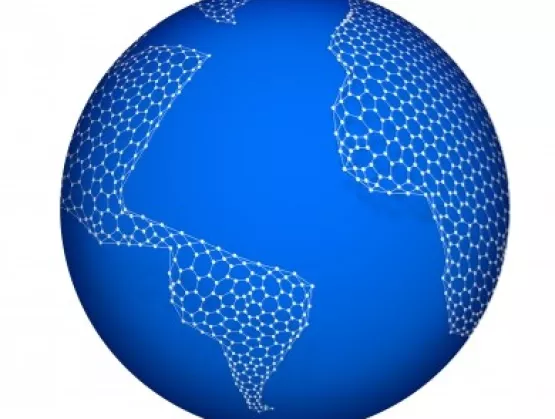
Materials science – a field that includes elements of applied physics, chemistry, and mulit-disciplinary engineering applied to magnetics, metallurgy, ceramics, polymers and silicon – serves as the foundation for technologies that have driven much of the tech sector’s economic growth for the past 50 years. As our devices grow smaller, faster and smarter – while also requiring higher performance and greater energy efficiency – we’re reaching the limits of what can be accomplished with these fundamentals. The technology sector needs renewed research and investment in new materials to help address the challenges we face in a rapidly changing world. Leading TDK Ventures, the investment arm of TDK Corporation, I’m happy to report that a number of young companies have stepped up to the challenge of innovating materials science for the 21st century. In the past 18 months, we invested in multiple startups dedicated to reimagining the basic building blocks of materials science and identifying new ways to push technology forward – in fact, three of them have successfully gone public or been acquired over the last year. This demonstrates not just a renewed interest in materials science research but also highlights the momentum for healthy returns on materials science investments. Or, as I like to say, it’s the return of materials science returns. Materials science at the atom level For high-tech investors, materials science went out of favor the past 10 or 15 years, because investment in software development companies began to deliver very healthy returns in relatively short time frames – often in as little as two or three years. Product development in materials science traditionally requires much more capital and takes a lot longer to generate returns than software startups. Today’s hardware innovators are making it clear that we’ve only begun to scratch the surface of what’s possible in the materials sciences. Unlike 20 years ago, we can develop products like graphene, which consists of a single layer of carbon atoms that is about 200 times stronger than steel and an excellent conductor of both heat and electricity. Nanometer-scale materials like this enable the design of ultra-low power, high-performance components that can integrate multiple functionalities onto very small devices and create opportunities that were impossible only a few years ago. With advances like this, the future of materials science is regaining its luster. Investors welcome materials science startups Three materials science startups with successful exits: GenCell, which went public in 2020, develops fuel cell solutions that offer clean backup power for a variety of commercial, industrial and healthcare operations and can be used for off-grid power and rural electrification in a wide range of temperature and humidity conditions. GenCell’s revolutionary process creates hydrogen-on-demand from anhydrous ammonia (NH3) at 10 times the efficiency of other solutions, without any outside electrical power.GenCell fuel cells enable hydrogen and oxygen to react in an emissions-free chemical process that produces electricity and heat, with pure water as the only by-product. Origin, acquired by Stratasys in 2020, creates 3D printer platforms that offer an additive manufacturing approach to mass manufacturing, with the freedom of open materials. Using Origin 3D printers, customers can print products of their own design from a range of materials, or from their own proprietary materials. Origin maintains strategic partnerships with the largest materials science companies in the world and print products for leading companies in the dental, medical, and industrial sectors. SLD Laser, acquired by KYOCERA in 2020, produced the world's first high-luminance, fully integrated white laser light emitter. The emitter is based on a gallium nitride solid-state laser projected through a high-performance phosphor element that converts the blue laser to broad-spectrum, incoherent white light that eliminates eye safety risks. The resulting light source emits 100x more luminance, projects 10 times the distance than an LED, and is being incorporated into a range of specialty, display and automotive lighting applications. Materials matter Many of the fundamental technological innovations of the last century, including advances in semiconductors, biotechnology, and server technology, were based on breakthroughs in materials science. At TDK Ventures, we believe the only way to advance further is to return to materials research to identify new ways to expand the horizons of science and technology. For some established companies, this may require a pivot from traditional ways of getting things done and embracing fresh ways of thinking. It means thinking more like a startup and welcoming the challenges of change and new opportunities. We also believe that these innovations should not just push the boundaries of existing disciplines but contribute to preserving our environment and improving the lives of people. This is one of the founding principles of TDK Ventures: Our investments must contribute to digital and energy transformation and help lead to a more sustainable world. Our goal is to help every startup we invest in achieve their full potential for positive world impact. For instance, GenCell fuel cells bring emissions-free electrical power to rural communities far from traditional electrical grids, helping raise living standards without reliance on polluting diesel generators. Laser lights from SLD Laser are more power-efficient than traditional LED lamps, as lights last over 10,000 hours longer than equivalent HID (high-density discharge) lamps. Origin 3D printer platforms enable safe, localized manufacturing, and are geared toward minimizing energy waste in the supply chain. We’re just scratching the surface of what’s possible with materials science. At TDK Ventures, we’re dedicated to delivering meaningful financial results while exploring the potential of new and transformative technologies to bring positive change to our society and environment. Nicolas Sauvage is managing director at TDK Ventures, the corporate venture capital (CVC) arm of Japan-headquartered electronics manufacturer TDK Corporation. TDK Ventures is a technology-focused venture fund, investing globally in early-stage startups that leverage fundamental materials science to bolster innovations in Digital Transformation (DX), Energy Environmental Transformation (EX), unlocking an attractive and sustainable future for the world.
Read More
Materials innovation has always been vital to the semiconductor industry. In the past, it was high-κ gate dielectrics. Today, Cobalt is seen as a replacement for Tungsten in middle-of-line (MOL) contacts.What materials innovation will the future bring?A likely answer is Graphene, the wonder material discovered in 2004.Graphene is one atomic layer of carbon, the thinnest and strongest material that has ever existed. It is 200 times stronger than steel and the lightest material known to man (1 square meter weighing around 0.77 mg). It is an excellent electrical and thermal conductor at room temperature with an electron mobility of ~ 200,000cm2.V-1.s-1. At one atomic layer, graphene is flexible and transparent. Other notable properties of Graphene are its uniform absorption of light across the visible and near infrared spectrum and its applicability towards spintronics-based devices.Graphene and Moore’s LawMoore’s Law scaling can be broken down into 4 key areas: Lithography FET Advanced Packaging (2.5D and 3D IC) Interconnect Material Solutions for upcoming nodes are starting to emerge in the first two areas (EUV and Nanowire- or Nanosheet-based FET respectively). Graphene play an important role in the latter two areas. For advanced packaging, Graphene can be used as a heat spreader (to lower overall thermal resistance), or as an EM shield (to lower crosstalk) as part of a 3D IC package.Active Graphene device layers can potentially be stacked on top of each other using a low-temperature transfer process ( 400°C) to allow for a dense heterogeneous “memory near compute” configuration. This is an area DARPA is actively researching as part of its new $1.5 billion Electronics Resurgence Initiative.Regarding interconnects, Copper interconnects are running out of steam and becoming a major IC bottleneck (projected 40% total delay for 7 nm node). Graphene’s high electron mobility and thermal conductivity make it an attractive interconnect material for MOL and back-end-of-line (BEOL), especially at line widths 30 nm.Graphene Device ApplicationsGraphene-based semiconductor applications are already starting to hit the market. A fully integrated optical transceiver (with a Graphene modulator and photodetector) operating at 25 Gb/s/channel was on display at the recent Mobile World Congress in Barcelona. San Diego-based Nanomedical Diagnostics is selling a medical device that uses a Graphene biosensor. Europe-based Emberion is building Graphene optoelectronic sensors that might find a home in LIDAR applications, where there is currently a focus on improving sensing in low-light conditions.What will the overall Graphene roadmap in the semiconductor industry look like? The history of ion implantation serves as a good example of how a fundamental scientific discovery moves from the lab to the foundry floor.The dominant view in the semiconductor industry at the time was that ion implantation would not work in practice (vs. thermal diffusion) and that, if it did, it would only marginally improve the manufacturing yields of existing products. There was nothing obvious about the transfer of ion bombardment techniques from nuclear physics research to semiconductor production.Varian (led by British physicist Peter Rose) built a new, advanced ion implant tool that Mostek (DRAM manufacturer based in Texas) was able to use to create MOS ICs with clear competitive advantages. The successful collaboration between Varian and Mostek was the turning point in the development of ion implantation as a major semiconductor manufacturing process. Over the next few years, semiconductor firms used ion implantation in a growing number of process steps and, by the late 1970s, it became one of the main processes used in semiconductor manufacturing.Likewise, the Graphene world needs to work closely with the semiconductor industry to develop the tools and techniques required to solve fundamental issues around Graphene growth (good uniformity over large area, low defect density) and Graphene transfer (high throughput, CMOS compatible). It is only then will we fully realize a future that includes 2D materials.The first step in this process is cross-industry education and initiating the dialogue between semiconductor industry and graphene companies. The National Graphene Association will be hosting the largest gathering of graphene companies and commercial stakeholders at the Global Graphene Expo Conference, October 15-17, 2018, in Austin, Texas.Learn more about graphene at the upcoming Global Graphene Expo Conference with dedicated panels of experts and investors, and roundtable discussions on how Graphene will impact the semiconductor industry. The event promo code is SEMINGA. About the AuthorAnand Chamarthy is the CEO and Co-Founder of Lab 91, an Austin-based startup that is working towards Graphene/CMOS integration at the foundry level. Anand can be reached at [email protected]. About the National Graphene AssociationThe National Graphene Association is the main organization and body in the U.S. promoting and advocating for commercialization of graphene and addressing critical issues such as standards and policy development.
Read More
Over the past three decades, most of the world’s innovations have centered largely on business models and involved iterative advances of existing technologies, with none matching the global impact of the top 10 semiconductor industry discoveries and advances, Dr. Morris Chang, founder of TSMC and the IC foundry model, said at SEMICON Taiwan 2018 this week.Few have as clear a perspective on the transformative power of semiconductors as Dr. Chang, founder of TSMC and father of the IC foundry model. Keynoting the IC60 Master Forum celebrating the 60th anniversary of the invention of the integrated circuit (IC), Dr. Chang listed what he considers the 10 key semiconductor industry innovation milestones since 1948:1. Invention of the transistor by Shockley, Bardeen, and Brattain – 19482. Silicon transistor – 19543. Integrated circuit – 19584. Moore’s Law – 19655. MOS technology MOS FET – 1964 Silicon gate – 1967 CMOS – 1970 6. Memory DRAM – 1966 Flash – 1967 7. Outsourced assembly and test (OSAT) – 1960s8. Microprocessor – 19709. VLSI systems design – 1970-1980 IP and design tools – 1980-present 10. Foundry model – 1985 Among the most consequential semiconductor advances may be yet to come, Dr. Chang said, citing innovations including artificial intelligence (AI) and machine learning, new device architectures, Extreme Ultraviolet lithography (EUV), 2.5D/3D packaging, and new materials such as graphene and carbon nanotubes.Dr. Chang argued that because bringing an innovation into production is immensely more expensive than proving a theory in a lab, innovators are not always the ones to implement and benefit from their novel ideas. Today, innovation costs are skyrocketing, driving more consolidation across the supply chain.Michael Droeger is director of marketing at SEMI.
Read More