downloadGroupGroupnoun_press release_995423_000000 copyGroupnoun_Feed_96767_000000Group 19noun_pictures_1817522_000000Member company iconResource item iconStore item iconGroup 19Group 19noun_Photo_2085192_000000 Copynoun_presentation_2096081_000000Group 19Group Copy 7noun_webinar_692730_000000Path
Skip to main content
Default Banner Image

Advantest

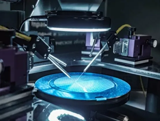
Artificial intelligence (AI) and high-performance computing (HPC) are driving unprecedented demand for data movement. As bandwidth requirements climb and conventional electrical interconnects encounter limitations in power consumption, latency and reach, silicon photonics, near-packaged optics (NPO), and co-packaged optics (CPO) are becoming increasingly important technologies for next-generation data centers.Much of the industry’s attention has focused on photonic device innovation. But demonstrating a high-performance photonic integrated circuit (PIC) is only part of the challenge. Turning these devices into products that can be manufactured reliably and economically at high volume requires a test infrastructure that can keep pace.This represents a significant shift. Semiconductor manufacturing has benefited from decades of refinement in automated electrical test. Silicon photonics adds an optical dimension that brings new requirements for fiber alignment, coupling efficiency, polarization management, and optical instrumentation—while still requiring conventional electrical characterization.As silicon photonics moves from development environments toward high-volume production, test becomes more than a quality gate. It is an integral part of the manufacturing strategy.An HVM-ready test solution requires a full complement of supporting hardware and software.Bringing precision optical alignment to productionOne of the most fundamental challenges is establishing a reliable optical connection to the device under test. Unlike electrical probing, where physical contact provides a relatively straightforward interface, optical testing depends on precisely coupling light into and out of very small structures.That coupling must be repeatable from device to device and wafer to wafer. Even small variations in fiber position or angle can affect insertion loss and measured optical performance, potentially making it difficult to distinguish actual device variation from variation introduced by the test setup.For this reason, high-volume testing requires automated alignment capabilities that can quickly locate the optical interface and optimize coupling. This can involve visual or image-based positioning to bring a fiber array unit close to the grating couplers, followed by area scans and gradient-search techniques to identify the optimal position via feedback loops – a technique typically referred to as “active alignment.” The process may also require optimization across six degrees of freedom—X, Y, and Z positioning plus three rotational axes—to maximize coupling efficiency and minimize channel-to-channel variation.The problem becomes more complex as optical interfaces add channels. Alignment must not simply maximize one channel's performance; it must produce consistent coupling across multiple channels. Rotational alignment, for example, can influence how evenly an optical beam overlaps multiple grating couplers. Other angular adjustments can affect both insertion loss and center wavelength.Polarization presents another variable. Because photonic structures can respond differently depending on the polarization state of incoming light, polarization must be characterized and controlled as part of a repeatable production methodology. Together, these requirements make alignment an active measurement and optimization process rather than a simple mechanical positioning step. The manufacturing challenge is to automate these functions without allowing alignment time to become a throughput bottleneck.Combining electrical and optical test without sacrificing throughputAlignment is only one part of the equation. A PIC may incorporate photodetectors, modulators, and other components requiring combinations of optical and electrical measurements. Typical characterization can include insertion loss, channel-to-channel uniformity, optical attenuation, photodetector responsivity, and wavelength-dependent behavior.Performing these measurements sequentially can add substantial test time. A more scalable approach is to integrate electrical and optical capabilities so that operations can occur concurrently wherever possible. For example, electrical alignment can occur before optical alignment, while continuity and other electrical tests may run during automated optical probe alignment rather than waiting for that process to finish. This type of parallelism becomes increasingly important as device complexity and test coverage grow.The same principle applies to optical instrumentation. Rather than treating each instrument as an isolated resource, high-volume environments benefit from integrated control of lasers, power meters, and other optical equipment, enabling parallel operation of multiple instruments or channels. Automated calibration and compensation are also important for maintaining measurement consistency as the test cell becomes more complex. Advantest’s development work in this area supports multiple optical instruments and parallel power-meter operation within a common test environment.The broader objective is familiar from semiconductor test: maximize useful test coverage while minimizing test cost. What changes with silicon photonics is the number of physical and measurement domains that must be coordinated to achieve it.Collaboration will be essential to ecosystem scalingNo single supplier controls all of the elements required for high-volume PIC test. The complete solution can span automated test equipment, wafer probing, optical positioning, fiber interfaces, optical instrumentation, device design, and manufacturing processes.That makes ecosystem collaboration particularly important. Test equipment providers need to work with probe and positioning specialists, photonic device developers, foundries, and manufacturers so the interfaces among these technologies function as an integrated production system rather than individual laboratory instruments.As an example, Advantest has collaborated closely with FormFactor to develop a wafer-level photonics test environment that combines electrical test instrumentation with wafer handling, optical instruments, and automated fiber alignment capabilities. The significance lies less in individual components than in the integration required to create a repeatable manufacturing workflow.As silicon photonics, NPO and CPO move toward broader adoption, these collaborative efforts will become increasingly important. The industry must develop practical test methodologies that accommodate evolving device architectures while delivering the repeatability, throughput, and economics expected of semiconductor manufacturing.Numerous photonics developments on the horizon will require broad industry effort to bring to fruition.The transition from promising photonic technology to high-volume commercial products will depend on more than advances in the devices themselves. Test must evolve alongside them. By treating optical alignment, electrical and optical measurement, automation, and ecosystem interoperability as parts of a single manufacturing challenge, the industry can build the infrastructure needed to bring silicon photonics fully into the era of high-volume production. About the AuthorDr. Clemens Leichtle is Senior Director and V93000 Photonic Business Lead for Advantest Corp. He has more than 25 years of experience in the semiconductor industry, with companies including Siemens, Agilent and Verigy, specializing in testing and developing respective application solutions for emerging technologies. For more than 15 years, he has been leading the V93000 Center of Expertise at Advantest; more recently, he co-led test solution development for silicon photonics and co-packaged optics targeting data center applications. Dr. Leichtle holds a Ph.D. in physics from the University of Ulm, Germany.
Read More
New SEMI Taiwan Testing Committee to strengthen the last line of defense to ensure the reliability of advanced semiconductor applications.Mobile, high-performance computing (HPC), automotive, and IoT – the four future growth drivers of semiconductor industry, plus the additional boost from artificial intelligence (AI) and 5G – will spur exponential demand for multi-function and high-performance chips. Today, a 3D IC semiconductor structure is beginning to integrate multiple chips to extend functionality and performance, making heterogeneous integration an irreversible trend. As the number of chips integrated in a single package increases, the structural complexity also rises. Not only will this make identifying chip defects harder, but the compatibility and interconnection between components will also introduce uncertainties that can undermine the reliability of the final ICs. Add to these challenges the need for tight cost control and a faster time to market, and it’s clear that semiconductor testing requires disruptive, innovative change. Traditional final-product testing focusing on finished components is now giving way to wafer- and system-level testing.In addition, the traditional notion of design for testing, an approach that enhances testing controllability and observability, is now coupled with the imperative to test for design, which emphasizes drawing analytics insights from collected test data to help reduce design errors and shorten development cycles. Going forward, the relationship among design, manufacturing, packaging, and testing will no longer be un-directional. Instead, it will be a cycle of continuous improvement.This paradigm shift in semiconductor testing, however, will also create a need for new industry standards and regulations, elevate visibility and security levels for shared data, require the optimization of testing time and costs, and lead to a shortage of testing professionals. Solving all these issues will require a joint effort by the industry and academia. "With leading technologies and $4.7 billion in market value, Taiwan still holds the top spot in global semiconductor testing market," said Terry Tsao, President of SEMI Taiwan. "When testing extends beyond the manufacturing process, it can play a critical role in ensuring quality throughout the entire life cycle from design and manufacturing to system integration while maintaining effective controls on development costs and schedules. Taiwan's semiconductor industry is in dire need of a common testing platform to enable the cross-disciplinary collaboration necessary for technical breakthroughs."The SEMI Taiwan Testing Committee was formed to meet that need, gathering testing experts and academics from MediaTek, Intel, NXP Semiconductors, TSMC, UMC, ASE Technology, SPIL, KYEC, Teradyne, Advantest, FormFactor, MJC, Synopsys, Cadence, Mentor, and National Tsing Hua University to collaborate in building a complete testing ecosystem. The committee addresses common technical challenges faced by the industry and cultivates next-generation testing professionals to enable Taiwan to maintain its global leadership in semiconductor testing.The SEMI Taiwan Testing Platform spans communities, expositions, programs, events, networking, business matching, advocacy, and market and technology insights. For more information about the SEMI Taiwan Testing platform, please contact Elaine Lee ([email protected]) or Ana Li ([email protected]). Emmy Yi is a marketing specialist at SEMI Taiwan.
Read More
From measurement equipment and components to medical devices, SEMI will showcase SMART technologies at its Smart Starts Here Pavilion, booth 40761, in the Smart Home section at CES, the world’s largest consumer electronics event. Do you want to discuss new technology directions and the latest developments in sensors, displays and electronics manufacturing? Hear about the new SEMI program that promotes “cool” careers in semiconductor manufacturing? Get the outlook for the manufacturing supply chain in 2019 and beyond?Stop by our booth or connect with any of our co-exhibitors in the Smart Starts Here Pavilion at booth 40731 in the Sands Expo Hall A. Co-exhibitors include:Advantest – A world-class technology company, Advantest is a premier manufacturer of measuring instruments used in the design and production of electronic instruments and systems. The company also focuses on research and development (R D) for emerging markets that benefit from advancements in nanotech and terahertz technologies and has introduced multi-vision metrology scanning electron microscopes essential to photomask manufacturing, as well as a groundbreaking 3D imaging and analysis tool.Altergy – Alertgy’s Glucose Monitor is a biosensor-based wristband device that provides non-invasive, real-time blood glucose monitoring for diabetics. The device gives both patients and healthcare professionals on-demand access to blood glucose levels via a smartphone application. C2MI – C2MI is the largest microelectronic innovation centre in Canada. Offering state-of-the-art equipment dedicated mainly to advanced packaging and microelectromechanical systems (MEMS), the centre hosts more than 250 R D scientists. Collaboration and synergy among our partners promote rapid commercialization of advanced prototypes.CHASM – CHASM Advanced Materials is a leading developer and manufacturer of printed electronics materials and battery materials based on proprietary carbon nanotube and ink/coating technologies.Kent Displays – Kent Displays is a global leader in unique eWriter display technology, with expertise in research, development, roll-to-roll manufacturing, and consumer packaged goods design and assembly using the eWriter technology. Kent displays also commercializes and sells the eWriter technology under its brand Boogie Board in a number of global retail markets. mCube – mCube makes the smallest motion sensors in the world. As a technology leader, mCube aspires to be the enabler for the Internet of Moving Things by putting a MEMS motion sensor on anything that moves. With over 500M units shipped, mCube continues to provide the world’s most advanced inertial sensors.Mitsui Chemical – Mitsui Chemical provides chemicals and gases for solutions in energy, agri-system, medical, IoT, and related fields. Mitsui specializes in advanced materials for automotive, ophthalmic lenses, dental, nonwovens, agrochemicals, and packaging. N5 Sensors – N5 Sensors manufactures chip-scale gas sensors that provides reliable gas detection in small-footprint packages. N5’s patented gas sensor technology represents a new era in low-power, microscale gas and chemical sensing that aims to replace conventional gas sensors. N5 is currently offering sensors and modules for integration. Its platform technology enables development of sensors for different gases ranging from toxics such as chlorine, nitrogen dioxide, to explosives such as hydrogen and methane, to environmental gases such as carbon dioxide.OMRON – OMRON Corporation is a global leader in the field of automation based on its core technology of "Sensing Control + Think." OMRON's business fields cover a broad spectrum, ranging from industrial automation and electronic components to automotive electronic components, social infrastructure systems, healthcare, and environmental solutions. Established in 1933, OMRON has over 36,000 employees worldwide providing products and services in 117 countries. In the field of industrial automation, OMRON supports manufacturing innovation by providing advanced automation technologies and products, as well as through extensive customer support, to help create a better society. PlayNitride – PlayNitride’s PixeLEDTM display can be used in addition to traditional displays. Focused on GaN-based MicroLEDs, PlayNitride, a fabless company, offers an innovative mass transfer process and SMAR.TechTM pixel repair technology. PlayNitride also provides a broad range of products and services including research and development in the field of compound semiconductors.Si-Ware - Si-Ware Systems' NeoSpectra specializes in the design and manufacturing of Microelectromechanical Systems (MEMS) powered miniature Fourier Transform InfraRed (FT-IR) spectrometers, or spectral sensors. Its sensors are affordable, robust, and easily adapted for a diverse range of industries.TEL - A leading global provider of semiconductor and flat panel display (FPD) production equipment, Tokyo Electron Limited (TEL) develops, manufactures and sales a wide range of products. All of TEL's semiconductor and FPD production equipment product lines maintain high market shares in their respective global segments. TEL provides outstanding products and services to customers through a global network of approximately 75 locations in 16 countries in the U.S., Europe, and Asia.ULVAC - ULVAC is a leading supplier of production equipment for the semiconductor, FPD and solar cell industries. Semiconductor products include MEMS release equipment, the ENTRON metallization system with PVD/CVD/ALD capability, etching systems for various applications including solutions for LED, power device and non-volatile memory. The systems and components are designed with innovative production technology for cost-effective device fabrication.Uneo - UneoTM offers high-quality sensor manufacturing services and product module design and consultation support to shorten product design cycles.Heidi Hoffman is senior director of Technology Communities Marketing at SEMI.
Read More