downloadGroupGroupnoun_press release_995423_000000 copyGroupnoun_Feed_96767_000000Group 19noun_pictures_1817522_000000Member company iconResource item iconStore item iconGroup 19Group 19noun_Photo_2085192_000000 Copynoun_presentation_2096081_000000Group 19Group Copy 7noun_webinar_692730_000000Path
Skip to main content
Default Banner Image

data center

The rapid growth of AI has created a surge in the global energy consumption at a rate never seen before. Today, data centers account for approximately 415 terawatt-hours (TWh) of electricity globally. To put this into perspective, the annual energy consumption of the United Kingdom in 2023 measured at 309 TWh. The International Energy Agency (IEA) projects data centers’ energy consumption will more than double to nearly 945 TWh by 2030 [1]. A single generative AI query can consume up to ten times the power of a traditional search [1]. Meanwhile, data center energy usage in the U.S. is projected to leap from 4.4% to as much as 12% of the national grid by 2028 [2]. This creates a stark reality for the semiconductor industry. Traditional monolithic scaling has hit its physical and economic limits, leaving advanced packaging and heterogeneous integration to define the industry’s trajectory [3].To meet these escalating compute demands, the industry is rapidly shifting toward multi-die architectures, chiplets, and 3D stacking to decrease the amount of energy needed for advanced computing. This transition is fueling explosive growth in the advanced packaging market, which the Yole Group projects will reach $79.4 billion by 2030 [4]. However, stacking chiplets to bypass Moore’s Law exposes massive systemic bottlenecks. Engineers are now fighting interconnect parasitics, navigating complex power delivery architectures, and battling extreme thermal density.In a 3D-stacked architecture, pulling heat away from vertically integrated dies is one of the most pressing engineering challenges of our time. As compute density rises, issues like die warpage and localized thermal hotspots threaten both reliability and yield. The shift toward sustainable AI systems for energy-efficient computing requires breakthroughs in everything from hybrid bonding process flows to advanced thermal interface material (TIM) strategies and liquid cooling integration [6].These are not challenges that any single company can solve in isolation. Whether you are a foundry, OSAT, material supplier, or equipment provider, overcoming these bottlenecks requires pre-competitive, industry-wide collaboration. Foundational capabilities must be built collectively before competitive differentiation occurs.This is the core mission of the SEMI Advanced Packaging and Heterogeneous Integration (APHI) Technology Coalition. By collaborating on common standards, shared research frameworks, cross-vendor interoperability models, and collective technology roadmap congruency, APHI is actively dismantling the barriers to next-generation computing.The APHI community is already tackling these issues head-on. Monthly chapter meetings identify and address these and other issues facing heterogeneous integration. The most recent chapter meetings showcased in depth review of these challenges. Jonathan Abdilla from BESI detailed the technical challenges and collaborative research required for global hybrid bonding process flows. Similarly, Dr. Jie Geng from Indium Corporation led a deep dive into crucial TIM strategies for AI and HPC, exploring hybrid stacking evaluation methods and liquid cooling options to combat GPU die warpage.The future of advanced manufacturing will be defined by how effectively we manage power and heat in heterogeneous systems. We invite you to join this critical conversation at the upcoming SEMIEXPO Heartland (April 29-30 in Detroit, MI) Day 2 will feature dedicated sessions on Thermal Management Power Delivery in Advanced Packaging: From TIMs to Warpage Control, as well as strategies for securing the advanced packaging supply chain.To help shape the standards and shared roadmaps that will power the AI revolution, explore our initiatives and get involved with SEMI Advanced Packaging and Heterogeneous Integration (APHI) Technology Coalition.Rafael Tudela is Senior Technical Marketing Manager at SEMI References[1] International Energy Agency (IEA). (2024). Energy and AI Report. [2] U.S. Department of Energy (DOE) Lawrence Berkeley National Laboratory (LBNL). (2024). Report on U.S. Data Center Electricity Demand and Grid Impact.[3] Semiconductor Packaging News. Advanced Packaging and Heterogeneous Integration. Retrieved from: https://www.semiconductorpackagingnews.com/articles/92402.html [4] Yole Group. (2025). Status of the Advanced Packaging Industry 2025.
Read More
Despite the pandemic lock-down, demand for electronic products and services remains strong. Work-from-home, video conferencing, and remote learning are driving data center growth and laptop and tablet demand. 5G infrastructure rollout is underway and smartphone sales are returning to normal levels. Automotive sales are increasing. At the same time, the industry is experiencing acute shortages of substrates. The October 2020 fire at Unimicron’s IC package substrate plant in Taiwan exposed the serious nature of the capacity shortage for IC package substrates. Substrate makers have been reluctant to make large investments in capacity over the last few years due to the fear that demand could decline and they would have excess capacity. Relentless price pressures by customers and the resulting low margins have weakened the finances of substrate suppliers. With tight capacity, substrate prices have increased and lead times are 14 weeks or more. The most critical shortage is for flip chip ball grid array (FC-BGA) substrates. In addition to increased demand in units, applications such as servers and networking products are seeing requirements for larger body sizes and increased layer counts. Shortages will not improve very soon because it takes time to build a new plant. And equip it. Key equipment for substrate production has lead times of up to a year. SEMI and TechSearch International detailed the substrate makers and provide projections for the substrate market, trends, and a list of suppliers and their plant locations in the Global Semiconductor Packaging Materials Outlook report. The report also highlights the market and suppliers for leadframes, bonding wire, encapsulation materials, underfill, die attach, solder balls, wafer level package dielectrics, and wafer-level plating chemicals. In times of shortages the report is an important indicator of suppliers in the industry and trends. Jan Vardaman is President at TechSearch International Inc.
Read More
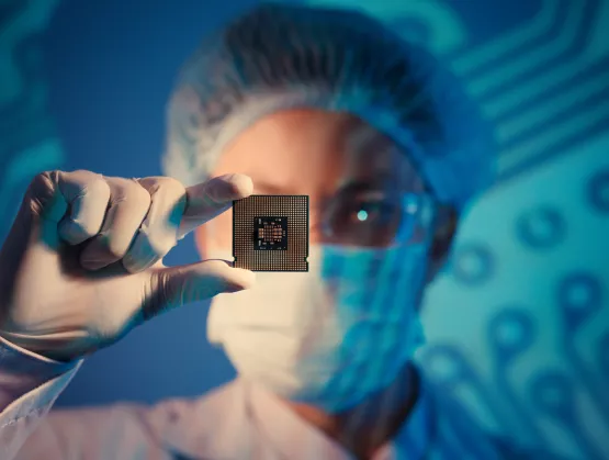
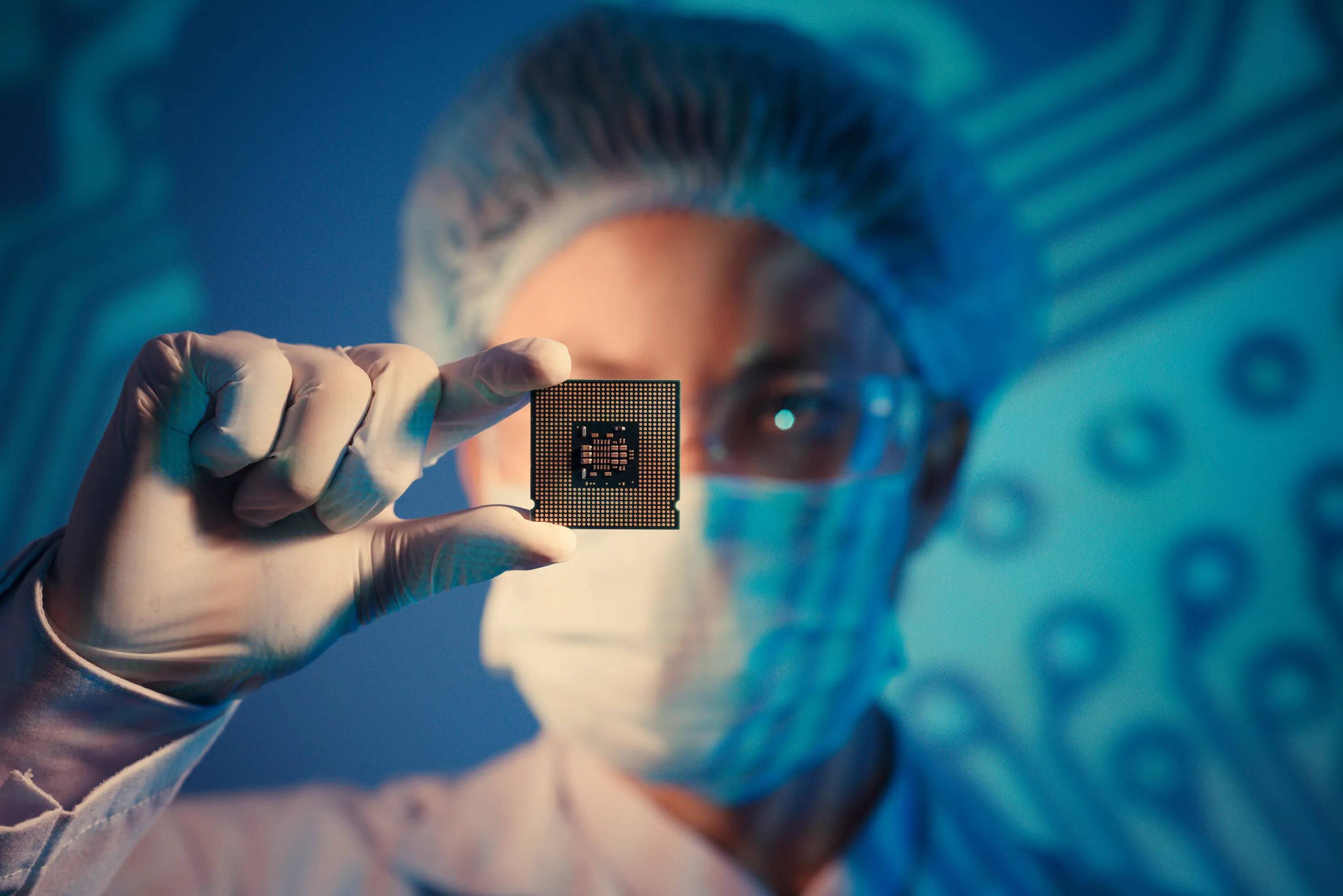
The more than 53,000 people who flocked to SEMICON Korea last month were treated to a motherlode of insight into the future of the semiconductor industry as 470 companies exhibited innovative technologies in more than 2,000 booths. But the annual event’s most arresting numbers came in keynotes and other presentations pointing to the extraordinary industry growth that lies ahead.“It is no exaggeration to say that 90 percent of the world’s data has been generated in the last few years,” said Jim Feldhan, president of Semico Research. “This explosive growth of data is expected to continue. That's why server shipments will grow by 20.3 percent, or 30 million units, this year alone.”Feldhan said that the Internet of Things (IoT) will be a chief driver of semiconductor industry growth, with IoT expected to be applied in areas as varied as automotive, smart cities, edge computers, finance, architecture, agriculture and healthcare. For its part, artificial intelligence (AI) will start to exercise human-like judgment. Feldhan noted that in many instances in these fields, “it is more accurate to apply AI and vision systems than to rely on traditional decision-making.”Yoon Jong Lee, senior vice president of DB HiTek, predicted that the Internet, AI and 5G will drive market growth. “Looking back over the past 30 years, semiconductor market growth was powered by PCs, the Internet and cell phones, yet last year memory accounted for 35 percent of total semiconductor sales, more than double the figure in 2016,” he said. He predicted that, in 2019, the foundry sector will outstrip the semiconductor market in growth, noting that the average growth rate of the semiconductor industry is expected to be 4.1 percent, compared to 7.1 percent for the foundry market. Clark Tseng, director of SEMI, reported that the strong semiconductor growth in 2018 is unlikely to continue in 2019 due to the decline in memory pricing, as well as mobile and PC demand. “Demand for semiconductors is likely to decline in the first half as the industry is still digesting inventory and rebound in the second,” Tseng said. Semiconductor industry growth headwinds include decreases in high-end smartphone purchases, PC demand and demand for DRAMs for servers in data centers, Tseng said. Declines in economic growth and consumption in China and the U.S.-China trade war will also contribute to a slowdown. However, Tseng noted that, over the long term, technology innovation will continue and that the semiconductor industry’s prospects remain bright.One key innovation will be the elimination of AI’s reliance on Internet connections in the future. In his opening day keynote, Eunsoo Shim, senior vice president at Samsung Electronics, emphasized that AI technology that operates without the Internet in the future is essential. “We are developing 'on-device AI' technology that incorporates AI algorithms in products such as smartphones and autonomous vehicles,” he said. "When on-device AI technology is implemented, it reduces reliance on the Internet, battery consumption, and data latency.” Reducing latency will significantly improve device response time.Walden C. Rhines, CEO Emeritus of Mentor, a Siemens business, predicted that AI will fuel rapid memory growth. The memory semiconductor (DRAM, NAND flash) market is expected to see a temporary slowdown this year, with the market expected to rebound in 2020. Rhines said that memory could be seen as an early market with rapid future growth, citing memory market super-booms in 1995 and 2000.“Memory production has not decreased since 1995 or 2000,” he said. “Although memory prices will temporarily fall this year after significant market growth in 2017 to 2018, the market will continue to grow as memory production increases,” he said. Rhines added that “although memory prices will drop by about 10 percent this year, he believes prices will increase 6 percent next year.” He also predicted the steady growth of the non-memory semiconductor market as AI technology matures and China’s investment in fabless companies continues.Indeed, SEMICON Korea speakers made it clear that concerns about the growth of the semiconductor industry are expected to be short-lived. While overall growth is likely to slow in 2019, the industry is expected to rebound steadily – powered by the semiconductor industry paradigm shift led by AI, IOT, and autonomous driving – and reach a new high of nearly $541 billion in 2020.Jaegwan Shim is a marketing specialist at SEMI Korea.
Read More
Korea is on track to top all other regions in fab investment, spending $63 billion between 2017 and 2020, with powerhouses Samsung Electronics Co. and SK Hynix leading the way, according to latest World Fab Forecast Report by SEMI. Samsung Electronics increased fab investments $770 million to $12 billion this year, and SK Hynix upped its spending a significant $2.8 billion to $7.25 billion in 2018.Korea's investment companies anticipate continued growth for both companies in the second half of 2018.Under this halo of extraordinary investment, nearly 380 SEMI Korea members and industry analysts gathered for 2018 SEMI Korea Members Day on September 13 to share insights on semiconductor market trends and new technologies that could help members bolster their competitiveness. Following are key takeaways from the event. Korea semiconductor market to grow 16% in 2018That’s according to IDC Korea VP Kim Soo-kyung, who noted that data center, memory and Internet of Things (IoT) are becoming key growth drivers for the semiconductor industry. He encouraged semiconductor companies to closely track development of automotive technology and the industry semiconductor market, both key growth areas. SEMI Korea president H.D. Cho opens SEMI Korea Members Day 2018 Continuing fab investment will lead to oversupply, but display will shineMarket entry by Chinese companies will also spur the oversupply, said Jeong Won-Seok, an analyst at HI Investment Corp. He noted that the oversupply will force Korea into stiffer competition with other regions. However, with OLED used for a wide variety of devices and the display industry seeing rapid growth, the sector will remain ripe for growth among Korean companies.Interconnecting various applications is a big semiconductor industry trendThe need for these interconnections will stand out in the mobility and high-performance computing (HPC) markets, said Park Sung-Soon, principal research fellow at Amkor Technology Korea, who addressed trends in packaging technology. He also emphasized interconnection cost efficiency as key to maximizing competitiveness.Smart Manufacturing is driving mass customizationAs semiconductor industry growth continues, production methods are shifting from ‘mass production’ to ‘mass customization,’ increasing the importance of Smart Manufacturing in driving greater production efficiency, noted BISTel VP Jeon Kyeong-Sik. Building a Smart Manufacturing platform to support large-scale production of specialized database and artificial intelligence (AI) chips will boost production efficiency, reduce costs and improve risk management. Virtual simulation will be a key enabling technology. SEMI analyst Clark Tseng presenting at SEMI Korea Members Day 2018 Surge in data volume and technology advances to drive long-term semiconductor industry growthThese key industry drivers will continue to power fab investment growth, with spending focused on 3D NAND, DRAM, and foundry, said Clark Tseng, director of Industry Research and Statistics at SEMI. China alone will see eye-watering growth with the region’s investments in domestic companies surging 46% from 2018 to 2019 and fab investment by Chinese domestic companies outpacing spending by foreign companies in China, Tseng predicted. SEMI membership rises with industry growthCulminating the event, SEMI Korea president H.D. Cho said, "With the growth of the semiconductor market, the number of SEMI members is gradually increasing, and we will help member companies grow with various activities such as Korea Members Day.”Jaegwan Shim is a marketing specialist at SEMI Korea.
Read More
SEMI Releases latest update to World Fab Forecast with adjusted semiconductor revenue consensus for second-half 2018 and 2019 Global semiconductor revenue in 2018 is now expected to reach $473.8 billion and clock a growth rate of 15 percent, a significant upward revision from the 7.5 percent expansion (to $442.9 billion) forecast at the start of the year by six research and investment forecasts tracked by SEMI Industry Research and Statistics (SEMI IR S). Data center growth will remain robust in the coming quarters, fueling demand for memory devices. In addition, cloud computing will continue to spur strong CPU, GPU, networking, ASIC, and DRAM and NAND demand through 2019, driving a consensus 3.63 percent year-to-year growth to reach the semiconductor revenue of $491 billion in 2019. Fab equipment spending (new and used) for 2018 is expected to increase by 14 percent to a record high of $63 billion, according to the last data from the SEMI World Fab Forecast, published by SEMI IR S. For 2019, fab equipment spending (new and used) is expected to increase 8 percent to another record of just under $68 billion. Memory continues to be the biggest swing factor in fab spending in 2018 and is expected to lead growth into 2020. 3D NAND will see the most capacity added in 2018 and 2019 with growth of 41 percent in 2018 and 27 percent in 2019, according to the SEMI World Fab Forecast. DRAM investment will see even stronger growth in 2018 and 2019 driven by new capacity addition as well as the continued technology shrink towards 1y/1z nm. For the first half of 2018, global spending for semiconductor fab equipment continues its growth momentum from 2017. Though we expect some softness in the second half of 2018, the outlook for 2019 remains robust with a fourth consecutive year of growth – the first such run since the 1990s. This prolonged growth cycle has been propelled by memory and will be extended by significant investment in China in 2019. Although a potential slowdown in 2020 is a concern, the overall outlook for semiconductor demand remains solid due to broad-based growth trends in data center, artificial intelligence (AI)/machine learning (ML), automotive, and industrial segments. Following are other SEMI forecasts for fab spending. Installed Capacity 3D NAND will see the most capacity added in both 2018 and 2019 with growth of 41 percent in 2018 and 27 percent in 2019. Foundry capacity growth is steady at 3 percent in 2018 and 6 percent in 2019, driven by both leading-edge and trailing-edge capacity buildup. 200mm fab capacity will increase 4 percent in 2018 and 3 percent in 2019, fueled by demand for MCU, sensors, PMIC, MOSFET and Driver IC. New Facilities / Construction Spending In 2018, there are 72 construction projects with investments totaling $15 billion, a year-over-year increase of 23 percent. Construction spending will reach all-time highs with China continuing its lead at US$7 billion in 2018, shattering its own record of $6.3 billion investment in 2017. Most construction spending in 2018 will be for Memory (just under $9 billion), primarily for 3D NAND followed by DRAM. Foundry will log second place in construction spending at just under $5 billion. Fab Equipment Spending Fab equipment spending (new and used) for 2018 is expected to jump 14 percent to a record high of US$63 billion, flat from the forecast issued in June 2018. Equipment spending (new and used) for 2019 is expected to increase 8 percent to another record of just under US$68 billion, a downward adjustment from +9 percent published in June 2018. We believe equipment spending will remain healthy, driven by solid, broad-based demand and predictable technology investments on top of constructive SEMICAP equipment fundamentals. Activity Report The August report features 1,265 records including about 300 Opto- and LED-related facilities. We have made 223 changes related to 216 fabs/lines. The modifications include the addition of new records, changes to existing records, the deletion of records since the February 2018 World Fab Forecast report. We are tracking 103 future facilities/lines with various probabilities that will start volume production in 2018 or later. Download a sample report Not a subscriber? Please review SEMI fab databases listed below. Our databases deliver the latest forecast and a complete analysis of front-end fabs and foundries worldwide. They are ideal resources to empower your market research. Eugenia Liu is a Senior Product Marketing Manager at SEMI.
Read More