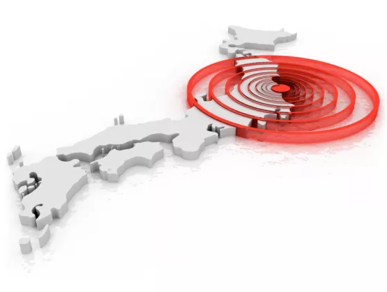
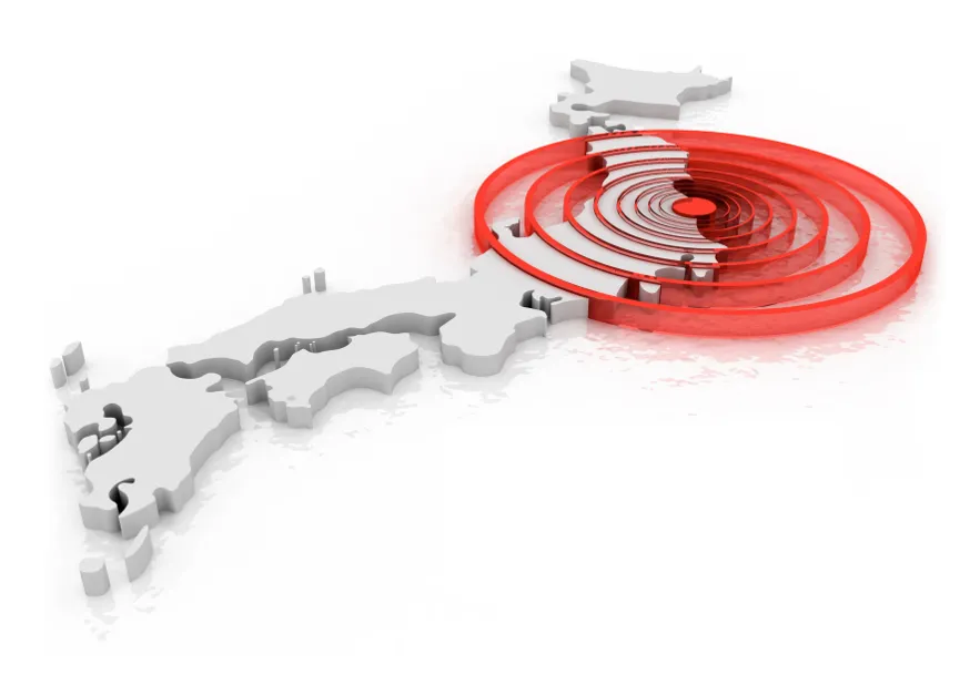
Famous for its warmth and hospitality, Japan always welcomes visitors from around the world with a gracious embrace. But when is the best season to visit? It depends on the interest of each visitor of course. For Instagrammers, the April cherry blossoms or November autumn leaves – a masterpiece of art with their rainbow gold, red and yellow hues – are ideal for snapping memorable pictures. For foodies, winter delights with tuna, toro sushi and other seafood at their tastiest. Wagyu peaks in richness, too, when the cold weather sets in. For anime and manga enthusiasts, August is definitely the time to visit. That’s when COMIKET, the world’s largest comic market – drawing more than a half million people – takes place in Tokyo. But for people in the electronics value chain, the perfect time to pack their bags and hop a flight to Tokyo is December, when SEMICON Japan – December 11-13 at Tokyo Big Sight – opens its doors with its own form of hospitality.Why should you attend? Here are the five top reasons.Reason 1: Japan is home to leading electronics industry suppliersAccording to VLSI Technology, seven of the top 15 semiconductor equipment suppliers in 2018 are headquartered in Japan, and many Japanese companies also lead backend equipment segments. For decades, Japanese companies have supplied about one third of the equipment for the global semiconductor equipment industry, according to SEMI and the Semiconductor Equipment Association of Japan (SEAJ). Most of these companies typically set up a booth on the SEMICON Japan show floor to welcome your visit.True, many Japanese suppliers also exhibit at SEMICON shows outside of Japan to meet with customers. But you will find many more engineers, managers and executives of equipment suppliers on their home ground at SEMICON Japan, where suppliers typically debut new equipment. Their booths are also ideal locations for visitors to meet with suppliers to ask questions, exchange opinions and negotiate new business deals.Japanese materials suppliers enjoy an even larger market share, providing about half the materials for the global semiconductor industry. These suppliers dominate in silicon wafers, photomasks, photoresists, sputtering targets, packaging substrates, bonding wires, leadframes, mold compounds and wafer level packaging dielectrics. Unlike equipment suppliers, not all materials companies exhibit. Instead, many participate as speakers and attend to connect with customers.Reason 2: Get ready for the next semiconductor industry upturnA year ago, in late 2018, we expected chip inventory to stabilize by mid-2019, yet the industry still struggles with high inventory overall and low average selling price for memory. The SEMI 2019 equipment billing forecast was lowered accordingly from -4.0 percent growth (2018 year-end forecast) to -18.4 percent (2019 mid-year forecast). However, the two forecasts still predict positive growth in 2020. As SEMICON Japan 2019 is underway, we should be at the beginning of the next upturn.The chart below shows that more wafer process fabs will start construction in 2020 than this year. (Please see article: Nearly $50 Billion in Fabs to Start Construction in 2020.) Custer Consulting Group also pointed to “a resumption in semiconductor chip and capital equipment growth in late 2019 or early 2020.” (Please see article: Semiconductor Industry Upturn by Early 2020?.)With better times ahead, SEMICON Japan 2019 will be an opportune time to exchange opinions with key players across the supply chain and start negotiations for the coming robust recovery of the equipment, components and materials markets.Reason 3: Glimpse the future at SuperTHEATERSEMICON Japan SuperTHEATER will feature industry and technology insights from global visionaries. Asako Eda, Japan’s chief representative officer of the World Economic Forum and the former president of Intel Japan, will open the SuperTHEATER with her keynote on how we live in an era where the fourth industrial revolution, climate change, disparity and geopolitical risks are affecting our lives and with the speed we have never experienced. She will explore the growing role of innovation and social responsibility and how the World Economic Forum is addressing associated challenges. The opening keynote session will also feature Nandan Nayampally, vice president and general manager of the Immersive Experience group at Arm.In all, the SuperTHEATER will host seven keynote forums over three days at SEMICON Japan including: Semiconductor Executive Forum – Terushi Shimizu, representative director and president of Sony Semiconductor Solutions, and Atsuyoshi Koike, president of Western Digital Japan, will discuss their business strategies and prospects. Manufacturing Innovation Summit – Executives from Applied Materials, KLA, Nikon and Tokyo Electron will discuss business and technology issues as well as innovations that will drive growth to 2030. All seven SuperTHEATER programs will be simultaneously translated to English for international audiences.Reason 4: Connect to application communitiesCollaboration across the value chain has never been more important to industry innovation and growth – the very reason SEMI has expanded its reach beyond the semiconductor manufacturing supply chain (equipment and materials) to include design, systems and products.The SEMICON Japan show and conferences will connect you to key application segments of the value chain. The SuperTHEATER will host two SMART transportation forums highlighting the latest developments in autonomous driving and sky transportation (flying cars). In the SMART Applications Zone on the show floor, you’ll find electronics products and technologies showcased for automotive and manufacturing automation as the autonomous driving pavilion highlights emerging technologies that are driving semiconductor innovation opportunities. Reason 5: Learn from disaster and recovery experiencesJapan has taken important disaster recovery lessons from devastating earthquakes over the past three decades, most notably the Kumamoto quake in 2016, the Tohoku temblor in 2011 and the Kobe rattler in 1995. So has the Japan electronics supply chain, including SEMI members. In the Business Continuity Plan (BCP) area at SEMICON Japan 2019, exhibitors including DISCO, Murata Machinery and THK will highlight technologies that can strengthen your preparedness for a disaster and aid in the recovery.On December 12 at the BCP seminar at Japan 2019, Sony Semiconductor Manufacturing, DISCO and Team Engineering Consulting will share their experiences and expertise in mitigating the disaster impacts. (Sony and Disco will present in Japanese.)To get the feel for the magnitude of a major earthquake and how seismic isolation protects against structural damage, be sure to take advantage of THK’s earthquake experience car. Seismic isolation installs isolators – rubber bearings, friction bearings, ball bearings, spring systems or other devices – beneath a building to buffer earthquake vibrations transmitted to structures.More reasons to attend SEMICON JapanAnd of course your visit to Tokyo for SEMICON Japan 2019 wouldn’t be complete without exploring Tokyo and other regions to experience Japan’s exotic culture, cityscapes and cuisine! Here are some resources to give you even more reasons to book a flight to Tokyo: Japan National Tourism Organization Go Tokyo Kyoto Tourism I look forward to seeing you at SEMICON Japan in December!Jim Hamajima is president of SEMI Japan.