downloadGroupGroupnoun_press release_995423_000000 copyGroupnoun_Feed_96767_000000Group 19noun_pictures_1817522_000000Member company iconResource item iconStore item iconGroup 19Group 19noun_Photo_2085192_000000 Copynoun_presentation_2096081_000000Group 19Group Copy 7noun_webinar_692730_000000Path
Skip to main content
Default Banner Image

SEMI Japan Members Day

Japan’s semiconductor industry has weathered the COVID-19 pandemic to post robust growth. Far from a temporary setback, COVID-19 will lead to enduring change in how we work and live. And just as automation has been a bulwark against the devastating business impacts of the virus outbreak, increasing digitization will lead to new efficiencies in our industry.These were some of the key takeaways from three SEMI Japan Members Day webinars in June and July that offered the latest updates on COVID-19 impacts to the semiconductor industry and restart strategies for SEMI members. More than 2,000 SEMI members across Japan’s islands attended the webinars featuring the following five speakers: Hideki Kanewaka, Marketing Director, Consulting Lead, Japan, Accenture Japan Ltd. Takayuki Komori, Manager, Marketing Engineering Dept, SUMCO Corporation Taketoshi Hamaguchi, Director, Manufacturing Industry, Microsoft Corporation Akira Minamikawa, Senior Consulting Director, OMDIA (Informa Intelligence LCC) Yuichi Koshiba, Managing Director Partner, Boston Consulting Group COVID-19 Impact on Japan Semiconductor Industry is ModestThe consensus view of the five speakers from various quarters of the industry – consultant, IT service provider, materials supplier, market analyst – was that the Japan semiconductor industry withstood the heavy blows COVID-19 dealt to other industries thanks to strong demand for chips. Shelter-in-place policies and lockdowns spawned by COVID-19 has accelerated the digital transformation rippling around the world as electronics sales have soared to support everything from remote work and education to healthcare and home entertainment including gaming.The rapid growth of cloud usage for video streaming, gaming and remote work is taxing communications network capacity and placing more bandwidth demands on servers, said Akira Minamikawa of OMDIA. According to a recent report by Nokia, communications network traffic has skyrocketed 300 percent for online meetings and 400 percent for gaming, bringing the networks closer to their capacity limits. Minamikawa sees server shipments increasing at 8 percent CAGR through 2024. For the broader chip market, he expects demand for notebooks, solid state and hard disk drives, and gaming to remain strong in 2020. He also predicts rapid 5G penetration for smartphones will boost semiconductor chip industry growth.Still, not all semiconductor segments are expanding, said Yuichi Koshiba of Boston Consulting Group. Chip shipments for end products in markets such as automotive, industrial equipment and aircrafts are on the decline. Slowing demand for chips that power automotive applications in particular could pare sales for some chip companies and distributors since the segment accounts for a high proportion of their overall revenue.State of the Semiconductor IndustryFrom SUMCO’s vantagepoint as a major silicon wafer supplier, the company’s Takayuki Komori sees a number of changes unfolding in the semiconductor industry: Smartphones are driving growing demand for process technology (smaller nodes) and 300mm wafers. Komori estimates the typical high-end smartphone sports 1,700 square millimeters of silicon. 300mm wafers account for 80 percent of that total while more than 50 percent of the devices use leading edge multi-patterning technologies. Smartphones will need more RF chips to support 5G’s high-speed communications and added frequency ranges. Substrates for RF switches and tuners have been shifting from gallium arsenide (GaAs) and other compound semiconductors to silicon. 5G smartphone penetration will accelerate as the cost of integrating CPUs and modem functions into a single chip sees a swift decline. While the sensitivity and resolution of CMOS image sensors have evolved to incorporate innovative backside illumination and stacking technologies, future advances will focus more on products for machine vision applications capable of sensing invisible light bands. Rising adoption of electric vehicles and robotics applications will drive growing demand for power semiconductors that control their motors such as IGBTs and MOSFETs as the production capacity for the devices expands and shifts to 300mm wafer lines. For memory fabs, Minamikawa said utilization remains high as a result of a spending slowdown by major chip manufacturers and will stay elevated even once additional capacity ramps to support robust demand. Foundry fab utilization also remains high despite the pandemic-driven cancellation of smartphone chip orders in March. Minamikawa also sees the utilization rate of micro rising with the surge in demand for notebooks, PCs and servers in the second half of 2020.Transition to New NormalAs people around the world start to settle into new ways of living and working, there’s a growing acceptance that the transformation will be long-lasting. And no area of people’s lives is changing more than their work. Boosted by government subsidies, many small and midsize companies in Japan have started to implement work-from-home policies, an area where major electronics and IT businesses had already instituted reforms, said Hideki Kanewaka of Accenture. A few examples: Nippon Telegraph and Telephone Corporation (NTT) announced that half of its employees will continue to work from home in the future. A five-year plan Toshiba launched in 2019 to allow all employees to work from home will likely accelerate. Hitachi plans to allow all employees to work from home starting in April 2021. dwango, a major internet-based entertainment company in Japan, announced it will allow in principle any employees to work remotely. In the critical area of remote sales, Kanewaka pointed to the importance of going beyond online business meetings, paperless transactions and virtual events to devise new ways to attract customers and close deals. Creating online communities and providing rich digital content are also important measures to consider, he said.Manufacturing's Digital TransformationTravel restrictions by most countries to curb the COVID-19 outbreak have also raised barriers to chip companies sending engineers overseas sites to service state-of-art equipment and provide other technical support. Microsoft’s remote assist system deployed by ASML is one tool semiconductor makers can use to overcome this challenge, said Taketoshi Hamaguchi of Microsoft.The system connects a remote equipment service expert with an onsite worker through the internet, allowing the technical expert to provide support through a goggle display with a camera worn by the worker. Guided by the expert, the worker can perform complex services. A Natural User Interface (NUI) helps give the factory worker a clear understanding of the often highly technical instructions.Using artificial intelligence (AI) to increase automation will also help reduce the reliance of semiconductor factories on onsite workers. For example, AI deep learning can be deployed to calibrate equipment autonomously and reduce downtime after scheduled maintenances, Hamaguchi said.Corporate Restart Strategies Beyond factory considerations tied to COVID-19, semiconductor companies will need to adapt their business strategies to new ways of operating. For example, global supply chains will shift to domestic sources and increase redundancy to ensure a steady supply, a change leading to higher overall costs, Koshiba said. Trade routes among regions will also be redrawn as the trade rift between the United States and China and other geopolitical tensions intensify. The total value of those routes is expected to recover by 2023.Koshiba advised companies to evaluate the supply chain trade-offs between stability and cost and factor in potential risks to improve their short-term resilience and drive mid- to long-term supply chain restructuring.After past recessions, 14 percent of companies restored sales growth, Koshiba said. He recommended investing aggressively in growth and seizing M A opportunities during the downturn. Chip companies must also adapt to supply chain changes faster than competitors.Become a SEMI MemberWebinars like the recent SEMI Japan Members Day series have become increasingly important in the mix of programs and services SEMI offers members to help them connect, collaborate and innovate in the microelectronics community. To become a SEMI member, please visit the SEMI website or contact your nearest SEMI office.Jim Hamajima is president of SEMI Japan.
Read More
Smart technologies have gripped the world’s imagination with their promise to revolutionize the way we live and work. With the semiconductor supply chain central to these advances, SEMI Japan in October hosted 200 members for SEMI Japan Members Day as speakers from three of the world’s top device manufacturers – Denso, Sony and Kioxia – offered their perspectives on the strides the semiconductor industry needs to make in three key areas: automotive, smart manufacturing and 3D flash memory manufacturing technology. Automotive Evolution and Electronics – DensoThe automotive industry is re-inventing itself to innovate across connectivity, autonomy, sharing and electric (CASE) and ensure safe, comfortable and environmentally friendly autonomous driving, said Nobuaki Kawahara, executive fellow and director of the Advanced Research and Innovation Center at Denso. Key focus areas of Denso in CASE innovation are Extraordinary Safety and Everyday Confidence. The company’s goal is to minimize damage to vehicles involved in collisions or one-car accidents by making it easier for drivers to detect and steer clear of objects in their path.To improve automobile safety and security, the company is developing advanced driver-assistance systems (ADAS) and autonomous driving technologies as it promotes the confluence of four areas of technology – HMI (Human Machine Interface), environmental recognition, vehicle control assistance, and information and communications. One use case Denso sees as a significant opportunity is deploying sensors such as millimeter-wave radar, cameras and LiDAR to monitor a vehicle’s surroundings, using GPS and precision mapping to pinpoint its location and determine the best route for safety and distance, and then transmitting that information to a motion-control system.Denso is also out to solve the hard challenges associated with autonomous driving in dynamic road conditions. Kawahara pointed out that road conditions vary and that rules for "driving at certain intervals in a certain lane" vary depending on the time of day. Also, on public roads in Abashiri, Hokkaido, where the company is currently conducting field tests, snowfall makes it difficult to recognize road images and gather sensor information. In Asia, it is also common for motorcycles and automobiles to speed along with very little space between them.Image Sensors to Accelerate Development of Smart Manufacturing – SonyTo fulfill the promise of smart manufacturing, the semiconductor supply chain must continue to invest in sensor and imaging technology innovation, said Shigeo Ohba, deputy senior general manager of the Imaging System Business Division at Sony Semiconductor Solutions. For its part, Sony is developing imaging sensors that help network and automate factories to achieve new production and cost efficiencies. For example, the company plans to design devices to increase equipment uptime through predictive maintenance, reduce defect rates and drive other manufacturing efficiencies. The challenge with today’s factory lines that produce a number of different devices is that they are highly complex to manage and therefore prone to human error, undercutting manufacturing efficiency. In the future, AI-powered machines will leverage data analysis to help streamline operations. Adapting an image sensor with AI to machine vision applications can simplify key processes such as measurement and inspection processes while reducing safety and security costs.Of the vast amount of information on all machines connected to the cloud, only essential details will be processed at the edge since edge data processing offers stronger security and reduces data transfer time. Ohba said image sensors will evolve based on edge AI, adding that "AI will be a paradigm shift for image sensors if it’s economically feasible."3D Flash Memory Manufacturing Technology Challenges – KioxiaIncreasing connectivity in factories for smarter, more efficient operations places huge demands on memory since networked devices typically store duplicate data, said Hideshi Miyajima, head of the Advanced Memory Development Center (AMDC) at Kioxia. To meet demand for higher networking speed and capacity, 2d NAND flash memory is moving to 3D and, in particular, three 3D techniques: multivalued memory, cell partitioning and layer stacking.To increase storage capacity, the third-generation 64-layer BiCS FLASH™ stacks layers to form nearly two trillion holes with a diameter of 100nm and a depth of 5μm on a wafer and places a uniform 2-3nm thin film on the inner wall of each 5-μm hole. For its BiCS FLASH™, Kioxia uses a dry etching technique that forms a straight, elongated through-hole and atomic layer deposition (ALD) technology, which creates a uniform laminate atomic layer on the wafer surface to grow materials uniformly and with high precision on large, complex substrates.In order to meet the cost expectations of high-volume 3D flash memory manufacturers, outlays across fabs must be reduced by better monitoring plasma control, enhancing yield through particle control, speeding film formation, and reducing gas, power and water usage, Miyajima said.SMART Transportation and SMART Manufacturing in the Spotlight at SEMICON JapanPlease join us at SEMICON Japan 2019, December 11-13 at Tokyo Big Sight, for the latest developments and trends in SMART Transportation and Smart Manufacturing. There are also a few other great reasons to attend. We look forward to seeing you in Tokyo!Jim Hamajima is president of SEMI Japan.

Read More
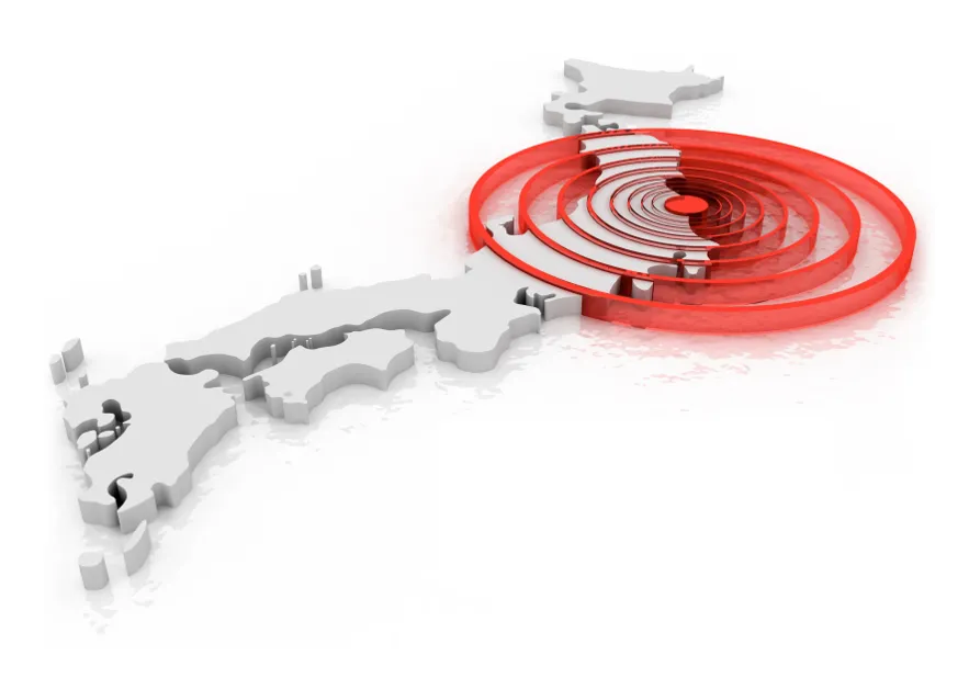
Wedged among four major tectonic plates, Japan is at the mercy of their abrupt herculean shifts and the earthquakes and tsunamis they can trigger. The fallout can be devastating. The magnitude 9 Great East Japan (Tohoku) temblor in 2011 and ensuing tsunami took nearly 20,000 lives, destroyed 138,000 buildings and cost $360 billion in economic damage.Factories including silicon wafer production facilities owned by Shin-Etsu Chemical and MEMC Electronic Materials – together accounting for 25 percent of the global silicon wafer production – sustained heavy damage. Operations were suspended. The Kumamoto earthquake in 2016 also caused significant damage. The economic cost: as much as $7.5 billion.With disaster risk rising on a global scale, these calamities offer valuable lessons in disaster preparedness and how companies can draw from their experiences to strengthen business continuity planning (BCP).Earthquake experiences and lessons in BCP were the focus of the recent SEMI Japan Members Day as speakers from five semiconductor device and equipment manufacturers offered their BCP strategies to about 150 SEMI members. Following are key takeaways from their presentations. Renesas: Create a robust production plant that is hard to break and easy to fixRenesas Semiconductor Manufacturing’s Naka plant took about 80 days to resume production while its ability to deliver semiconductors was delayed even longer as it recovered from damage caused by the Tohoku earthquake, said Yoshiyuki Miyamoto, Representative Director and President at Renesas. Operations at the company’s Kawajiri plant were disrupted by the Kumamoto earthquake.A key lesson from both earthquakes: The company needed to promote risk visualization from top-to-bottom in the supply chain. With the goal of making its plants easy to repair but hard to break down, Renesas implemented a risk management plan for earthquake preparedness plan to ensure stronger production line resistance and a stable supply to customers. The company ran simulations of multiple earthquake scenarios including aftershocks, enabling it to develop new BCP training and preparedness measures. Sony: Staying transparent about the disaster, sharing and interacting with related companiesYukihide Keigo, a representative from the Sony Semiconductor Manufacturing, showed footage taken the day the Kumamoto earthquake damaged a production line at its Kumamoto Technology Center. Sony is the top manufacturer of imaging sensors worldwide, and the Kumamoto plant is the backbone of that production. The magnitude of the foreshock fell within levels Sony had accounted for in its BCP at that time, and the line was expected to return to full production within a week. However, the magnitude of the earthquake that followed outstripped expectations, and the company’s BCP didn’t hold up. Three and a half months later, the plant had finally fully recovered. The protracted recovery prompted Sony to develop an earthquake preparedness plan using a model that assumed double the magnitude of expectations. For full restoration, the company identified challenges to returning to full operation at each stage of the production line. Then it went even further, developing in-house diagnostics, implementing critical path methods and strengthening earthquake resistance of equipment that manages bottlenecks for the restart of the plant. The revision of its BCP plan led to the establishment of a system to shorten the resumption of production after a major earthquake to just two months.Sony shared the contents of its BCP review with other companies to solicit help identifying any gaps and highlighted its partnership with Renesas in the Semiconductor Industry Association in Japan (JSIA), a committee of the Japan Electronics and Information Technology Industries Association (JEITA), to share materials procurement resources for the purposes of disaster preparedness and business continuity. HORIBA STEC: Steady daily practices protect hundreds of millions of yen worth of products HORIBA STEC’s Aso plant, near the epicenter of the Kumamoto earthquake, suffered heavy damage that cut off electricity and the water supply, yet production in its clean room resumed in just 10 days, said Hiroyuki Koyama, a factory manager at the plant. The plant’s quick recovery stemmed from daily preventive measures implemented before the quake such as connecting freestanding shelves for greater stability, applying thick rubber bands as rails to prevent manufactured goods from falling to the floor, and placing equipment on rolling carriages instead of fixed shelves.The practices saved the Aso plant hundreds of millions of yen in products and materials that otherwise could have been lost in the earthquake. Koyama also offered the reminder that, with regulations governing factory layout and construction differing widely depending on factors such as a building’s age, companies need to tailor their BCPs to the unique characteristics of each building. THK: The key point of dampening earthquakesTHK’s ACE Division develops earthquake dampening and vibration control devices designed to absorb the vibrational energy of an earthquake, though the devices must also be designed for precise analysis of that energy, said Hidemi Murao. Murao provided an overview of the latest technologies and products for dampening earthquake vibrations and shared test results from experimental devices.Murao described how THK’s recently introduced Linear Motion (LM) Guide, an earthquake vibration dampening technology, can significantly reduce building vibrations during a temblor. In a video Murao showed to demonstrate how the guide works, a shelf loaded with equipment rests on a platform equipped with THK’s LM Guide equipment. Simulating an earthquake, the platform shakes vigorously in every direction but the shelf remains steady as the LM Guide dampens the vibrations. The platforms can be installed on floors or underground in buildings or factories to prevent shelves from toppling. Tokyo Electron: The ideal BCP management systemOne risk associated with BCP training is that it can become overly routine, dulling the response of employees in actual disasters, said Tokyo Electron Vice President Tatsuya Aso. To help keep its workers’ skills sharp, TEL held surprise drills with employees assigned to particular BCP roles to test their ability to adapt quickly to when disaster strikes. In addition, TEL has launched surveys in more than 70 overseas locations to optimize safety in these high-hazard facilities.The SEMI Japan Members Day presentations made clear that the issue of BCP transcends boundaries between individuals, manufacturers, regions, and sectors within the global electronics supply chain. Disaster preparedness requires problem-solving across the entire supply chain, with companies sharing technical knowledge, offering mutual aid, and striving for continual improvement. Collaborative is essential. At SEMICON Japan 2019, SEMI will continue to bring companies together to address BCP initiatives and share their technical knowledge with members. Jim Hamajima is president of SEMI Japan.
Read More