downloadGroupGroupnoun_press release_995423_000000 copyGroupnoun_Feed_96767_000000Group 19noun_pictures_1817522_000000Member company iconResource item iconStore item iconGroup 19Group 19noun_Photo_2085192_000000 Copynoun_presentation_2096081_000000Group 19Group Copy 7noun_webinar_692730_000000Path
Skip to main content
Default Banner Image

U.S.

AEM Holdings Ltd, a Singapore-based multinational corporation, is listed in Forbes Asia’s 200 Best Under A Billion 2019 and 2020 spotlighting small and midsized companies in the Asia-Pacific region with sales under $1 billion. AEM clinched the Singapore Business Review Technology Excellence Award 2020 for Analytics-Semiconductor and the Singapore Business Awards Enterprise Award 2019/2020. These achievements are testament to AEM’s vision and innovation and the company’s contributions to the increasingly complex testing of chips in a rapidly evolving technological world. I spoke with AEM CEO Chandran Nair, a new Regional Advisory Board (RAB) member of SEMI Southeast Asia, about the company’s intelligent test and handling solutions, its role in digital transformation, the company’s key role in the smart manufacturing movement and the growth prospects for Singapore’s electronics sector. SEMI: AEM’s application-specific, intelligent system test and handling solutions for semiconductor and electronics companies serve the advanced computing, 5G and AI markets. How do you differentiate your solutions from those offered by competitors? Nair: A key differentiation for AEM is that we work closely with our customers to develop application-specific integrated test and handling solutions that meet their needs in a scalable manner from lab to production. We offer our customers customized, full-stack test and handling solutions that give them the agility to accelerate their delivery cycles and enhance product quality. Over the years, AEM has developed and acquired world-class technologies in instrumentation, test, automation, robotics, optical inspection, high-end thermal control, and software. These technology pillars, along with our deep know-how to customize test and handling solutions using the technology pillars as a platform, enable AEM to meet the fast-changing needs of our customers faced with the challenges of testing heterogeneous and complex devices. In addition to investing in technology, AEM has also invested in delivering application-specific solutions to meet customer demand. Our recently announced acquisition of CEI with its manufacturing capabilities in Vietnam and its specialization in low-volume, high-mix manufacturing increases our geographical reach and our ability to quickly turn application-specific test and handling solutions to be deployed. We have a unique and differentiated approach that enables our customers to test high-performance computing devices, automotive devices, and mobility devices with maximum test coverage, cost-effectively, in a manufacturing environment. Our experience in serving the high-performance computing market that traditionally drives advancements in thermal control also puts us at the forefront of delivering comprehensive thermal management, vision, and deep automation and test solutions for the computing, automotive, and mobility markets. AEM also has a strong instrumentation portfolio, including high-density digital instruments and mixed-signal and protocol-aware instrumentation that is well-suited for ATE solutions for SoC, high-power devices, and CMOS image sensors. Over the last few years, we have also established leadership positions in developing and deploying application-specific test solutions for MEMS devices and offering wafer and frame probing stations suitable for R D, wafer sort, and final test. We form strong partnerships with our customers, provide them with end-to-end support in product development, and take them through the entire life cycle process from concept to mass production. Chandran Nair and Goh Meng Klang, vice president of operations, at the AEM manufacturing site in Singapore. (Photo credit: AEM) SEMI: Digital transformation is powering strong growth of advanced computing, 5G and AI. Will AEM be expanding its AEM manufacturing plants in China, Malaysia and Singapore to meet rising demand for these technologies in the coming years? Nair: In regards to manufacturing, AEM currently has manufacturing facilities in Singapore, Malaysia, the U.S., Finland, and China. With our recently announced acquisition of CEI, we will add manufacturing capability in Vietnam and Indonesia. AEM will continue to expand manufacturing appropriately to give our customers cost-effective solutions while maintaining our proven track record of delivering on time and scaling rapidly in times of crises like the pandemic or geopolitical disruptions. As for advanced technologies, the three key factors that will bring the full potential of 5G to fruition are 1) cost-effective, high-powered processing devices at the edge, 2) easy access to high-bandwidth communications, and 3) cost-effective sensor technology. Semiconductors are the primary drivers of these three key success factors. As devices become more complex and our reliance on semiconductor-powered devices in all aspects of our lives deepens exponentially to include mission-critical applications, AEM’s role is to ensure that our customers' electronic and semiconductor devices are shipped thoroughly tested, safe to use, and highly reliable. It is imperative that, as a testing company, we find innovative ways to help our customers test their products with maximum coverage and minimum cost. To do this, we are focusing our R D efforts and investments to continue building on our key technology pillars to ensure that we stay ahead of the curve when it comes to test and handling solutions. We prepare our customers to test increasingly complex devices manufactured on the latest process node. SEMI: During your career you’ve driven projects in test and automation and more recently robotics solutions for ports, logistics warehouses and transport. With robotics and automation a key part of Industry 4.0, what role do AEM solutions play in powering the smart manufacturing movement? Nair: The smart manufacturing movement is powered by semiconductors, software and increasingly by artificial intelligence (AI). Test is at the heart of the process of ensuring that semiconductor and electronics devices reach the consumer well-tested for reliability. With our vision of enabling A Zero Failure World, AEM addresses the necessity for safe, highly reliable devices. The semiconductor companies themselves are adopting smart manufacturing methods. AEM’s tools are Industry 4.0-ready, and we continue to invest in machine learning and data analytics, which are integral to the future of test. Our tools are automated and feature embedded sensors to provide our customers with data about tool usage, the state of a machine’s health, and more. Our tools are connected to our customers’ manufacturing automation platforms. Additionally, we continue to invest in our ability to better slice and dice test data to understand trends and patterns to help our customers analyze data and make decisions faster. SEMI: You also have experience heading autonomous vehicle projects. With the COVID-19 pandemic hastening digital transformation, do you see an acceleration in the development of fully autonomous vehicles and smart manufacturing? Research and development efforts for autonomous vehicles (AV) continue at a fast pace worldwide. With shutdowns and restricted movement rules globally, the pandemic has hastened digital transformation in many ways. The delivery of goods and services is transforming, and AV will surely play a part, especially in secure environments for autonomous transport. The pandemic has accelerated the development of autonomous vehicles and smart manufacturing technology in automation-friendly environments like factories and ports. SEMI: At the recent Global Technology Summit hosted by SEMI, you spoke about testing innovations to meet the demands of highly complex devices. Please elaborate on innovative testing solutions versus traditional testing? Nair: AEM offers a disruptive and differentiated solution, one that is driving a paradigm shift to asynchronous, modular, highly parallel, smart testing solutions. ​ The traditional approach of ATEs to test increasingly complex devices on advanced nodes has reached a point of diminishing returns as it gets exponentially more expensive to increase test coverage to acceptable levels. Additionally, as devices get more complex and companies are rapidly adopting heterogeneous packaging technologies, the realization that System Level Test (SLT) is necessary is forcing a rethink of the entire test process. AEM’s provides asynchronous, modular, highly parallel test cell solutions that enable each test cell to run SLT, final test, or burn-in all in one system and its ability to handle hundreds of test cells independently with each test cell testing multiple devices. Our solutions suddenly make comprehensive testing of every complex device cost-effective. Freeing us from legacy ATE allows AEM to provide these innovative solutions to our customers. AEM engineering and manufacturing teams in Singapore at work on semiconductor test and handling systems for global deployment at world-class semiconductor facilities. (Photo credit: AEM) SEMI: Singapore seems to be in the sweet spot of digital transformation. Singapore’s industrial production grew 8.6% year-over-year in January 2021, an expansion driven mainly by a surge in sectors including electronics, and more growth is seen in the year ahead. Digital technologies such as 5G technology and cloud computing together with continued demand for work-from-home equipment is behind this growth. What are the growth prospects for the region’s electronics sector? Nair: Singapore is well-poised to benefit from the current digital transformation accelerated by the adoption of these technologies during the pandemic. Being a safe, well-governed country with strong IP protection, excellent infrastructure, and the rule of law, Singapore is in a great position to play a central role in cloud-based services, 5G, and the semiconductor industry. Singapore’s semiconductor sector output is at a record high, and the prospects for renewed growth in the region are very good. SEMI: As a new Regional Advisory Board member of SEMI Southeast Asia, how is your industry experience relevant to the scope of this role? What opportunities lie ahead for the region? Nair: I am honored to represent AEM in the SEMI’s Southeast Asia RAB. The SEMI RAB can influence policymakers with ideas and information on the current and future needs of the industry. I also believe that SEMI Southeast Asia can cultivate a strong innovative semiconductor ecosystem that helps regional and global growth. I look forward to working with other very experienced and accomplished board members. Bee Bee Ng is president of SEMI Southeast Asia.
Read More
The COVID-19 pandemic has inflicted major impacts on manufacturing operations worldwide including in the semiconductor industry. The virus has left millions of people confined to their homes, resulting in a massive shift to virtual work and online engagement. In Singapore, where AEM is headquartered, our management team took proactive measures to protect our workers by implementing best practices ahead of the Singapore Circuit Breakers.AEM is globally deemed an essential service, requiring us to maintain operations and minimize impact to our customers. Business continuity plans that include work-from-home and safe-distancing guidelines are in place. As of the time of this writing, we are very fortunate that all of our employees are safe and that we’ve seen only minimal impacts to our customer commitments. AEM has confined this impact by spreading operational risks across our facilities in Asia, Europe, the U.S. and divisions in Singapore, Malaysia, China, North America, Central America, Finland, France and Vietnam. All told, these facilities employ more than 550 people (Figure 1).Figure 1 – AEM Global Presence As a global leader, AEM offers application-specific intelligent system-level test and handling solutions for semiconductor and electronics companies that serve the advanced computing, 5G communications and artificial intelligence (AI) markets.Leveraging our decade of experience, the latest AMPS solutions provide asynchronous, modular, massively parallel and smart system-level testing to meet the new test challenges of complex ICs. The modularity and scalability of these systems enables customers to scale their existing engineering device validation solutions into high-volume, massively parallel production solutions that increase faults coverage, reduces time to market, and decreases cost of test and ownership (Figure 2).Figure 2 – AMPS System-Level Test Solution In meeting 5G infrastructure test needs, AEM developed a field-deployable fiber optics tester. Called WideOptix SR4, the system was initially developed in collaboration with a world leader to support the 5G fiber infrastructure deployment in China and has now been adopted for some Ethernet standards testing. With our WideOptix SR4 development, we cultivated Silicon Photonics (SiPh) testing expertise that complements our AMPS system-level test capability. As part of our business continuation and risk diversifications plan, we had also set up factories in Penang (5,200m2) and Suzhou (3,600m2). Penang’s rising influence in the Southeast Asia semiconductor industry has prompted AMM (AEM Malaysia) to expand its scope to include value-added services with a Center of SSD Excellence and Center of Photonic Excellence.ASZ (AEM Suzhou) will continue to focus on the domestic market in China for further expansion and penetration with products ranging from cost-sensitive testers to state-of-the-art test measurement instruments. In Europe, AEM is focused on wafer-level test and cost-effective ATE test solutions. Finland-based AFORE specializes in MEMS and application-specific wafer testing with the ability to add physical stimulus. The company's state-of-the-art instruments enable the testing of devices such as diced IMU’s (Inertia and Motion Units) in continuous rotation on a wafer mounting ring. Our process increased test throughput by 3X compared to the traditional pick-and-place methods (Figure 3).Figure 3 – Wafer-Level Test Throughput Advantage A specialist in application-specific wafer handling, AFORE developed its latest design to support quantum computing in collaboration with its partner BLUE FORS. The company’s probing equipment features a handling solution with temperature tolerances to 2K (-270’C) to support cryogenic testing (Figure 4).Figure 4 – Cryogenic Quantum Computing Probing Solution AFORE also gained critical insights into creating total darkness, enabling us to further explore opportunities for dark matter testing. AFORE is currently in talks with a member of the LUX Photonics Consortium funded by the National Research Foundation (Singapore) to provide a dark body testing environment and handling for its IR detectors.In Europe, our acquisition of Mu-TEST in France helps diversify our product and service offerings while spreading our business continuity risks. Mu-TEST enjoys collective test-development experience of more than 320 man-years thanks to various ATE suppliers including Schlumberger and Credence. To help combat rising costs of traditional ATE, Mu-TEST developed cost-effective solutions using FPGA-based instruments supported by a full suite of test development, debug and production test software with links to EDA and standard interfaces. This provides Mu-TEST an agile platform that can be easily re-configured for different customer needs.This Mu-Test acquisition expands AEM’s system-level testing capability to include Functional Test, allowing BIST, SCAN, JTAG to test structural failures and perform other application-level test that interface directly with the DUT using the EVM (Electronics Validation) boards to increase fault coverage within the same test environment. Mu-TEST has also enabled AEM to form the recent partnership with UTAC to develop a cost-effective CIS test solution that addresses UTAC’s test needs and complements its CIS advanced packaging solutions. Our U.S. headquarters based in Chandler, Arizona has expanded its capabilities to provide application engineering.In summary, AEM has been expanding its global footprint while managing risk and has been fortunate to be positioned to manage the recent COVID-19 excursions. While each geographical location specializes in core technologies, all sites have access to one another’s manufacturing facilities in times of need and a pool of IP available to address new opportunities. We believe this risk diversification positions us well to serve the needs and interests of our customers worldwide.Lo Wee Tick is Director, Business Development, and Stuart Pearce is Senior Director, Field Marketing, at AEM Holdings Ltd.
Read More
On Monday, SEMI led a statement from a coalition of industry groups calling on governments worldwide to harmonize their policies to safely allow essential international travel by essential workers. Cross-border mobility in the semiconductor and microelectronics industry is vital to maintaining manufacturing critical to the production of semiconductor devices that are the foundation of our modern economy, countless economic sectors and each nation’s response to the COVID-19 pandemic. Uniform cross-border travel rules impacting essential businesses in the electronics supply chain are crucial for semiconductor business infrastructure and supply chains to maintain effective operations.To that end, SEMI is urging governments around the world to permit international travel by semiconductor supply chain engineers, technicians and executives with minimal disruption to ensure any fast-tracked procedures apply directly to the semiconductor industry and that any agreements negotiated among countries harmonize global travel procedures and processes. Global supply chains require cross-border travel by key technical personnel and business continuity decision-makers to ensure that essential industry manufacturing and business operations remain efficient, effective and uninterrupted. While the industry continues to implement safety protocols and minimize non-essential travel to stem the spread of COVID-19, highly sophisticated equipment sets and materials usage from multiple nations will at times require specialized expertise that is not present in-country.For example, technicians from a semiconductor manufacturing equipment company typically must travel to semiconductor factories in other countries to install or repair specialized tools in situations that are beyond the expertise of the local field office and too complicated to handle by video conference. Similarly, at times semiconductor-based solutions, such as cloud computing, must be implemented or optimized on-site for the equipment to achieve full capacity. After months of remote access to their overseas operations, it also is critical that executives are able to visit their facilities to evaluate and manage their ongoing operations. In the past month, several countries central to the global electronics supply chain have engaged in both formal and informal talks to ease travel restrictions on personnel from essential industries. China, for example, is negotiating fast-track travel protocols with countries throughout Asia and Europe. On May 1, China and South Korea formalized an agreement that has made significant accommodations for semiconductor industry personnel to travel between the two countries. Last week, China and Singapore reached a similar deal – planned to take effect in early June – prioritizing travel for both executives and technicians.Beyond China, several ad-hoc negotiations are underway involving countries as varied as Taiwan, Vietnam, South Korea, Thailand, Canada, Australia and New Zealand. Multilateral discussions are also afoot with the aim of setting up bubble travel zones featuring standard health and travel protocols within the country blocs. As these disparate agreements between individual countries or small blocs of countries take shape, however, they are likely to create divergent standards that may complicate efforts of global businesses to effectively service their operations and customers, even if such travel is and has been deemed essential.In March, when U.S. states and many governments around the world began implementing stay-at-home orders and closing non-essential business operations, SEMI immediately took a lead role advocating to ensure that that the entire microelectronics supply chain was deemed essential and able to continue operations. In the U.S., nearly every state followed SEMI’s recommendation to adhere to the Department of Homeland Security’s Cybersecurity and Infrastructure Security Agency (CISA) guidelines that included semiconductor manufacturing and its supply chain as essential, or specifically highlighted semiconductor supply chains as essential. Overseas, SEMI advocacy worked to ensure the semiconductor supply chain was deemed essential in every key jurisdiction.The mobility of essential workers is critical to essential business operations in the electronics supply chain. Just as SEMI led the effort to ensure that critical electronics supply chain operations were deemed essential as economies were closing down, SEMI will continue to advocate for uniform essential travel guidelines for critical infrastructure workers as economies reopen. Karl Kailing is manager of Public Policy and Advocacy at SEMI.
Read More
By many measures, South Korea is swiftly restoring life as usual after suffering a heavy COVID-19 caseload in March. The region has logged an average of about 10 new COVID-19 cases per day since mid-April, it enjoys an ample supply of facial masks and sanitizer, and the Korean government on May 6 lifted social distancing orders and now encourages routine distancing to keep the coronavirus at bay. South Korea is also making progress on the business front as regions including China, Vietnam, Poland, Hungary and Kuwait have started to crack open the doors for travel by Korean businesspeople. As of mid-May, more than 5,500 Korean workers had received permits to travel to the five nations. For several months, South Korea was subjected to international travel bans to stem the spread of the coronavirus. Then, as its COVID-19 case count dropped, other nations started to loosen their bans on business visits to South Korea. In mid-May, the Korean government won work-related travel privileges to Vietnam for 186 Samsung Display engineers, while some LG engineers were also granted the travel permits.Other steps forward for the Korean microelectronics supply chain include the following: About 1,150 workers from Samsung, LG group and affiliates subject to a 14-day quarantine were granted entry to Vietnam 340 employees from 143 small and midsize Korean companies traveled to Vietnam under a 14-days quarantine 252 LG Group workers won fast-track entry to Nanjing, China 215 Samsung Display, Samsung SDI and Samsung Electro-Mechanics engineers were permitted entry to Tianjin, China under the region’s fast-track program 170 LG Display workers with fast-track privileges flew to Guangzhou, China 300 Samsung Electronics workers arrived in Xian, China via fast track Shanghai, Tianjin, and Shandong are among 10 provinces in China that have implemented the fast-track entry program. South Korea businesspeople are required to follow a number of protocols to help ensure the safety of China’s citizens such as: Submitting to temperature checks at least 14 days before departure and COVID-19 tests within 24 hours of leaving South Korea Showing health certificates that they have tested negative for COVID-19 Undergoing COVID-19 testing once they arrive in China. Workers testing negative for the virus can start work within three days. Other regions are also weighing a loosening of travel restrictions to South Korea. For example, the Japan government is considering issuing business travel permits to 10 countries including Korea, China, and the United States. The start to re-opening international borders to business travel is a promising step toward restoring the global collaboration and connection at the heart of the microelectronics industry. Jaegwan Shim is a marketing specialist at SEMI Korea.
Read More
In an important step toward resuming business as usual in Japan, Prime Minister Shinzo Abe on May 14 lifted the state of emergency originally scheduled to expire at the end of May for 39 of Japan’s 47 prefectures, marking “the real beginning of our efforts toward a new normal in the era of the coronavirus” as new cases continue to decline. But with Tokyo, Osaka and six other prefectures still under the state of emergency, Abe urged citizens to remain cautious as the nation and world continue to confront the COVID-19 threat. Among criteria the remaining prefectures must meet for a state of emergency suspension is a reduction in new infections to no more than 0.5 cases weekly for every 100,000 citizens. The eight prefectures account for nearly half of Japan’s population and GDP, with Tokyo and Osaka the two largest urban areas in the island nation. Japan expects to contain its economic losses to 38 trillion yen, 15 percent less than the 45 trillion yen hit originally projected. The Japan government has planned a May 21 progress review[1] in the eight prefectures, a timeline that Abe said could lead to the lifting of the state of emergency before the original cutoff at the end of the month, a move that would help stem the drain on the domestic economy.Strict Immigration Controls Restricts International Travel to and from Japan by Supplier EngineersAs I reported on April 21, the Japan Foreign Ministry on March 31 raised its travel advisory to level 3 for 49 regions around the world including the U.S., prohibiting travel from Japan for any purpose. SEMI Japan is urging government officials to exempt Japanese supply chain engineers from the travel ban to allow visits to semiconductor manufacturing facilities in those regions in order to install, start up and service equipment.Starting May 14, Japan blocked immigration of foreign nationals and permanent residents from 100 countries and regions worldwide, a ban applying to anyone who spent time in their home region within 14 days of their planned arrival in Japan. The areas include China, Singapore, South Korea, and Taiwan in Asia; Canada and the U.S.; and Germany, France, Italy, Netherlands, Switzerland and the U.K. in Europe. For the complete list, see the Japan Ministry of Justice’s website.Japan’s immigration ban mirrors restrictions now in place in many other regions around the world. The immigration controls are well-intended – to restrict the spread of COVID-19 – but hamstring the global microelectronics supply chain. For example, the curbs bar engineers from international travel to install new tools and software in fabs. SEMI Japan has stressed the potential chip industry impacts of the ban in ongoing talks with the Ministry of Economy, Trade and Industry and is facilitating discussions between government representatives and SEMI members to help clear the way for travel by critical supply chain workers to Japan. SEMI Supports Members with COVID-19 ResourcesSEMI international headquarters and regional offices are here to help you, our members. For more information on our webinars, surveys, best practices and other information designed to help you meet the challenges of the pandemic, please visit the SEMI Coronavirus Updates Resources page.[1] The May 21 review found three prefectures in western area – Hyogo, Kyoto and Osaka – met the criteria to lift the state of the emergency. Four other prefectures – Chiba, Hokkaido, Saitama and Tokyo – remain under the emergency order that will be reviewed again as early as May 25.Jim Hamajima is president of SEMI Japan.
Read More
In much of post-lockdown China, urban life is humming. The streets of Beijing and Shanghai are bustling with traffic, smog again shrouds city skylines with the resurgence of economic activity, property sales are bouncing back and a revival in consumer confidence is taking hold. Emerging from monthslong shelter-in-place orders, the nation has seized a large measure of control in containing COVID-19 as it breaks fertile new ground in pandemic response and recovery. 
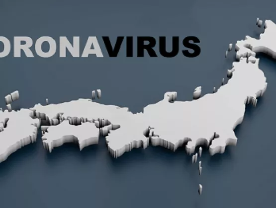
In Wuhan, Hubei, the fountainhead of the novel coronavirus, one company offers a striking example of China’s muscular COVID-19 containment efforts, carefully continuing to operate through January and February as the virus set root, said Karel Eloot, a Shenzhen-based senior partner and Asia leader of Transformation and Operations practices at McKinsey Company, speaking at a recent webinar presented with SEMI. Soon, COVID-19 spread to eight other provinces that suffered serious outbreaks and forced the nationwide lockdown that sent China’s GDP plunging 7 percent, its first contraction in 28 years. An impressive array of safety protocols, many designed to reduce people density as a bulwark against the virus, animates China’s fight against COVID-19, a return-to-work movement that is laying a path forward for companies around the world. It is these measures, Eloot said, that have kept the Wuhan company afloat and helped other businesses across China restore operations with unusual speed. Community and Social Distancing – The Heart of China’s COVID-19 Response In establishing safeguards, many companies started by assessing staffing requirements, identifying workers essential to sustaining on-site operations while allowing others, such as white-collar staff, to work from home, though some have since returned to their offices. Seen as non-essential, some factory maintenance workers have been instructed to stay home. To fill staffing gaps, business have turned to multi-skilling practices, such as having on-site supervisors and engineers step out of their daily roles to handle lower-level operations activities. Much of the focus has been on community distancing, with businesses quickly identifying workers suffering even minor COVID-19 symptoms and using contact tracing to prevent sick or vulnerable employees from entering offices and factories and turning them into hot zones for community spread, Eloot said. Manufacturing facilities are staggering work shifts to reduce people density, closely monitoring workers’ body temperatures with an eye toward other symptoms, and following up with medical tests and quarantines as needs dictates. QR codes, long a staple of e-commerce, have been a particularly effective weapon in combatting COVID-19. Companies are deployed the scanning technology to identify workers by color code – green, yellow or red – and assign various levels of site access depending on who they’ve been in contact with. Some factory workstations are now walled off by transparent plastic sheeting to prevent COVID-19 infection through aerosol drift. In business meetings and lunchrooms, staffers sit spaced a safe distance apart and facing the same direction to avoid crosscurrents of the microscopic respiratory droplets that can carry the virus. Others eat in isolation. Meeting room windows are opened, weather permitting, to admit fresh air. And elevators – perfect petri dishes for contagion – are shuttered to ward off human clusters, shifting all floor-to-floor movement to staircases. Companies united by the common goal to keep goods flowing through supply chains are providing masks and other personal protective devices to smaller players most vulnerable to the economic shock of COVID-19. The aim: Shield the companies from the potentially crippling effects of the virus to avoid supply chain breakdowns that can undercut the performance of the whole. Even competitors have formed unexpected alliances, sharing parts and components that are in short supply. “Some sectors have maintained steady production throughout the crisis” thanks to these practices, Eloot said. “China has been able to create safe communities where people can operate as normal.” Executive Uncertainty Reigns, Hope Springs Eternal with Innovation The objective of China’s fast, forceful response to the COVID-19 outbreak is economic: A V-shaped rebound after the 7 percent wallop to its GDP in the first quarter of the year. The trajectory is among nine economic recovery scenarios McKinsey Company presented to more than 2,000 executives worldwide in a recent survey seeking their views on the likelihood of each. The business leaders coalesced around two – a full restoration of global GDP growth that could materialize this year or extend into next, or a two- to three-year recovery following the initial economic tsunami, Sven Smit, an Amsterdam-based senior partner with McKinsey and global leader of the McKinsey Global Institute and global COVID-19 response team, said at the webinar. The executives see the multi-year recovery as the most likely. The shorter rebound ranked second on a scale of probabilities. Notably, the business leaders found the V-shaped bounceback China is attempting – returning to GDP growth in one quarter – the least likely outcome. But the biggest surprise from the survey, Smit said, was executives’ view that of the two major global interventions for restoring GDP growth – viral and economic – one will be ineffective, reflecting their deep uncertainty about what lies ahead. A growing body of knowledge about COVID-19 tempers that doubt. It’s established fact that the virus is highly contagious, more lethal than the flu, and spread by means including aerosols and touching contaminated surfaces. But only recently has more insight emerged about human immunity. Broad-based blood testing in the Netherlands has discovered that only 3 percent to 4 percent of the people screened are immune to the coronavirus, leaving the vast majority of the population without natural biological protection – a sweeping vulnerability evident in Asian countries hit early by the virus only to see fresh flare-ups after initial containment. Smit warned of the pandemic’s potential resurgence. Testing has revealed that coronavirus cases are underreported by a staggering 10- to 15-fold, a clarion call that countries “need to be very careful about how they re-open economies.” That means in order to keep COVID-19 at bay until a vaccine is developed, the best defenses will remain temperature monitoring, contact tracing, quarantining, social distancing, mask wearing, frequent hand-washing and other proven protective measures. And while the relative contribution of each safeguard to slowing COVID-19’s spread is unknown, Japan, Korea, China, Taiwan and other Asian countries have shown that “if you apply them all, you are likely to keep this virus under control,” Smit said. It remains to be seen whether protections the U.S. and European countries have put in place will stave off the virus as effectively as the rigorous measures implemented by Asian countries and, if the Western regions deploy a different cocktail of safety protocols, how well they will work. The re-opening of their economies promises to reveal the answers – and the McKinsey recovery scenario they’ll face. These and other open questions help explain the uncertainty of the executives McKinsey polled. Pandemic Supercharges, Adds New Urgency to Long-Term Trends What is known is that, far from upending the way all organizations operate, COVID-19 is supercharging secular trends and showing that people can react with dizzying velocity when confronting global mortal threats. That speed, Smit said, “is not determined by the potential of technology, but by events." For decades, doctors and technologists have teamed to develop ways to examine and treat people from afar, yet telemedicine managed to eke out only small, incremental gains in adoption. Since the COVID-19 outbreak, patients have flocked online, with virtual doctor’s visits accounting for more than 70 percent of all physician-patient interactions. “People like it, and we can reach many more patients as a result. It happened in a few weeks,” Smit said. Similarly, teachers and unions have only inched toward digital communications for years, fearing job losses in education at the hands of technology. When schools closed recently under shelter-in-place orders, teachers quickly switched to online lessons. The transition, Smit said, took one weekend. Meanwhile, as office workers holed up at home, usage of teleconferencing applications skyrocketed. “We’re collectively learning at unprecedented speed,” Smit said. “We’re sharing. We’re learning about supply chains. We’re learning about collaboration. We’re learning about masks. We’re learning about contact tracing. We’re learning how to work more efficiently. We’re learning from real-time data about the behavior of people. And we’re investing collectively enormous sums in finding cures and treatments and expanding hospital capacity.” While the coronavirus’s blistering spread caught many countries off-guard, Smit expects scientists to spare no effort to innovate. Expressing hope that new medical interventions will be available by summer, Smit said the world needs to buttress its key lines of defense against the coronavirus until a vaccine is developed – a shield that will quicken the global economic recovery. “The race is on," he said. Related blog COVID-19: Economic and Microelectronics Industry Impacts – Insights from McKinsey Company For McKinsey’s latest insights on the coronavirus pandemic, visit its website, which is updated daily. For the latest COVID-19 information and SEMI event updates SEMI is providing members, visit Coronavirus Resources. Michael Hall is a marketing communications manager at SEMI.
Read More
Japan’s Prime Minister Shinzo Abe declared a state of emergency for Tokyo, Osaka and five other prefectures[1] on April 7 in response to a startling increase of COVID-19 infections in the region’s cities in an uneasy moment for its domestic semiconductor industry. The declaration, effective through May 6, authorized the six prefectural governors to strengthen curbs on the spread of the virus and included guidance for citizens to stay home and restrictions on operations of non-essential businesses.With Japan supplying some 40 percent of the world’s chip production equipment and materials, the declaration stirred fears among semiconductor manufacturers that their uninterrupted operations – critical to sustaining the global industry – might be at risk. Japan Government Designates Semiconductor Industry as EssentialIn April 7 and 11 revisions to its Basic Policies for Novel Coronavirus Disease Control, the Japanese government allayed those concerns by designating semiconductor manufacturers essential businesses – a stark acknowledgment of the chipmakers’ vital role in combatting the novel coronavirus. The policy stated:“Among medical and manufacturing industries, we request the continuation of the following business operators in consideration of infection prevention: operators who are difficult to stop production line due to the characteristics of the equipment (such as blast furnaces and semiconductor factories); and operators who produce essentials (including important items in supply chains) for protection of the people who need medical care and support, as well as for maintenance of social infrastructure. We also request the continuation of the business operators who sustain medical care, the lives of the people, and maintenance of the national economy.”[2]SEMI Japan Reaches Out to Prefectures to Urge Essential Business Designation Equipment and materials shortages can halt production of an entire fab line and ripple through intricately connected global supply chains to stifle the production of end devices including the electronics critical to COVID-19 treatments. Electronic devices also play a central role in containing the virus’s spread by enabling artificial intelligence (AI), data analytics, digital communications, telemedicine, robotics, remote health monitoring, telecommuting, online shopping and other digital services.The essential business designation was explicit recognition that Japan’s semiconductor supply chain is integral to the global chip production ecosystem and worthy of the same protections the government has implemented for semiconductor companies. With SEMI members operating in Japan’s 47 prefectures, I sent letters to all prefectural governors three days after the second policy revision, urging them to apply the same designation, and the SEMI Japan team is following up to secure their support.SEMI Japan Encourages Government to Exempt Members from Travel Restrictions The Japan Foreign Ministry on March 31 raised to level 3 its travel advisory for 49 regions including the U.S., China, Taiwan and South Korea, encouraging Japanese citizens to avoid travel regardless of purpose to blunt the international spread of the coronavirus. SEMI Japan is working with the Semiconductor Equipment Association of Japan to urge the government to exempt semiconductor supply chain companies from the level 3 travel restrictions if they implement measures to prevent domestic infections and contagion in the visited regions. The exemptions would allow supply chain companies to install and service equipment at fabs – one key to maintaining smooth, uninterrupted operations.SEMI Supports Members with COVID-19 ResourcesSEMI international headquarters and regional offices are here to help you, our members. For more information on our webinars, surveys, best practices and other information designed to help you meet the challenges of the pandemic, please visit the SEMI Coronavirus Updates Resources page.[1] The six prefectures are Tokyo, Kanagawa, Chiba, Saitama, Osaka, Hyogo and Fukuoka.[2] Provisional translation by Ministry of Health, Labour and Welfare. Full document is available at https://www.mhlw.go.jp/content/10900000/000620733.pdf.Jim Hamajima is president of SEMI Japan.
Read More
Today, the U.S. Trade Representative (USTR), as part of its Section 301 investigation into China's trade practices, released a list of approximately $300 billion worth of Chinese goods, including a number in the semiconductor supply chain, that would face a tariff of up to a 25 percent. SEMI is working with members to assess the industry impact and will submit written comments and testify against the tariffs at a public hearing scheduled for mid-June.SEMI encourages members to review the new list and determine the level, if any, of impact.Today’s announcement follows last Friday’s tariff hike from 10 percent to 25 percent on $200 billion of imports from China. All told, the U.S. already has levied tariffs on $250 billion of Chinese goods that include materials and machines critical to semiconductor manufacturing. The expanded list released Monday would impose tariffs on essentially all imports from China. For its part, China has announced retaliatory tariffs, but more are likely coming.SEMI has been steadfast in its opposition to these tariffs and other barriers to global commerce. Over the past year, SEMI has submitted numerous written comments and offered testimony on the damaging impact of tariffs to the semiconductor industry. While SEMI strongly supports efforts to strengthen intellectual property protections, we believe that the tariff increases will do nothing to address concerns over China’s trade practices but, instead, harm companies in the semiconductor supply chain by increasing business costs, introducing uncertainty and stifling innovation.SEMI will continue tracking ongoing trade developments. SEMI members with questions should contact Jay Chittooran, global public policy manager at SEMI, at [email protected].
Read More
Yesterday, President Trump extended the deadline for List 3, which would have raised U.S. tariffs on $200 billion worth of goods from China. SEMI welcomes the deadline extension.Over the past three months, the United States and China have engaged in bilateral discussions to address structural issues like intellectual property protection and requirements for the use of joint ventures as well as trade balance concerns. President Trump announced that these talks have yielded significant and substantial progress in all areas. That said, it’s been reported that discussions on structural issues, such as forced technology transfer, have seen limited progress.Certainly, questions remain on the specifics of liberalization, the structure of the agreement and, most notably, enforcement. Any new commitment will be toothless without a firm and binding enforcement mechanism. While the date of the new deadline hasn’t been clarified, we believe that the tariffs won’t be increased before Presidents Trump and Xi meet, which could happen in late March at Mar-a-Lago.List 3 covers a range of items, including a number of consumer goods, but also directly impacts items critical to the semiconductor manufacturing process, including materials and machines. SEMI estimates that all U.S. and Chinese retaliatory tariffs – which hit machines and tools central to the semiconductor industry, including equipment used to manufacture wafers, boules, and chips as well as test, inspection and sensing equipment – will cost members more than $700 million in annual duties.While SEMI strongly supports stronger protections for valuable intellectual property (IP), tariffs will not help address Chinese trade practices and will ultimately have significant and unintended consequences. SEMI asserts that these tariffs will harm companies in the semiconductor supply chain by increasing business costs, introducing uncertainty, and stifling innovation. The tariffs seem to target U.S. firms for simply operating in China.Given that chips, tools, and materials are extremely complex, precise, and difficult to manufacture, it is not reasonable to believe that any component can easily be replaced with a part from another source. Further, this U.S. government approach does not take into account that many items subject to these tariffs are not available, at sufficient quality and cost, from domestic sources, or even non-Chinese sources. We stand steadfast in our belief that this trade action will raise prices, put thousands of high-paying and high skill jobs at risk, and curb growth.SEMI will continue monitoring new developments in this area. Any SEMI members with questions should contact Jay Chittooran, Global Public Policy Manager at SEMI, at [email protected].
Read More
The more than 53,000 people who flocked to SEMICON Korea last month were treated to a motherlode of insight into the future of the semiconductor industry as 470 companies exhibited innovative technologies in more than 2,000 booths. But the annual event’s most arresting numbers came in keynotes and other presentations pointing to the extraordinary industry growth that lies ahead.“It is no exaggeration to say that 90 percent of the world’s data has been generated in the last few years,” said Jim Feldhan, president of Semico Research. “This explosive growth of data is expected to continue. That's why server shipments will grow by 20.3 percent, or 30 million units, this year alone.”Feldhan said that the Internet of Things (IoT) will be a chief driver of semiconductor industry growth, with IoT expected to be applied in areas as varied as automotive, smart cities, edge computers, finance, architecture, agriculture and healthcare. For its part, artificial intelligence (AI) will start to exercise human-like judgment. Feldhan noted that in many instances in these fields, “it is more accurate to apply AI and vision systems than to rely on traditional decision-making.”Yoon Jong Lee, senior vice president of DB HiTek, predicted that the Internet, AI and 5G will drive market growth. “Looking back over the past 30 years, semiconductor market growth was powered by PCs, the Internet and cell phones, yet last year memory accounted for 35 percent of total semiconductor sales, more than double the figure in 2016,” he said. He predicted that, in 2019, the foundry sector will outstrip the semiconductor market in growth, noting that the average growth rate of the semiconductor industry is expected to be 4.1 percent, compared to 7.1 percent for the foundry market. Clark Tseng, director of SEMI, reported that the strong semiconductor growth in 2018 is unlikely to continue in 2019 due to the decline in memory pricing, as well as mobile and PC demand. “Demand for semiconductors is likely to decline in the first half as the industry is still digesting inventory and rebound in the second,” Tseng said. Semiconductor industry growth headwinds include decreases in high-end smartphone purchases, PC demand and demand for DRAMs for servers in data centers, Tseng said. Declines in economic growth and consumption in China and the U.S.-China trade war will also contribute to a slowdown. However, Tseng noted that, over the long term, technology innovation will continue and that the semiconductor industry’s prospects remain bright.One key innovation will be the elimination of AI’s reliance on Internet connections in the future. In his opening day keynote, Eunsoo Shim, senior vice president at Samsung Electronics, emphasized that AI technology that operates without the Internet in the future is essential. “We are developing 'on-device AI' technology that incorporates AI algorithms in products such as smartphones and autonomous vehicles,” he said. "When on-device AI technology is implemented, it reduces reliance on the Internet, battery consumption, and data latency.” Reducing latency will significantly improve device response time.Walden C. Rhines, CEO Emeritus of Mentor, a Siemens business, predicted that AI will fuel rapid memory growth. The memory semiconductor (DRAM, NAND flash) market is expected to see a temporary slowdown this year, with the market expected to rebound in 2020. Rhines said that memory could be seen as an early market with rapid future growth, citing memory market super-booms in 1995 and 2000.“Memory production has not decreased since 1995 or 2000,” he said. “Although memory prices will temporarily fall this year after significant market growth in 2017 to 2018, the market will continue to grow as memory production increases,” he said. Rhines added that “although memory prices will drop by about 10 percent this year, he believes prices will increase 6 percent next year.” He also predicted the steady growth of the non-memory semiconductor market as AI technology matures and China’s investment in fabless companies continues.Indeed, SEMICON Korea speakers made it clear that concerns about the growth of the semiconductor industry are expected to be short-lived. While overall growth is likely to slow in 2019, the industry is expected to rebound steadily – powered by the semiconductor industry paradigm shift led by AI, IOT, and autonomous driving – and reach a new high of nearly $541 billion in 2020.Jaegwan Shim is a marketing specialist at SEMI Korea.
Read More