downloadGroupGroupnoun_press release_995423_000000 copyGroupnoun_Feed_96767_000000Group 19noun_pictures_1817522_000000Member company iconResource item iconStore item iconGroup 19Group 19noun_Photo_2085192_000000 Copynoun_presentation_2096081_000000Group 19Group Copy 7noun_webinar_692730_000000Path
Skip to main content
Default Banner Image

Cadence

In the early 1990s, engineers of varying degrees of skill with a powerful PC set up shop designing and selling blocks or libraries of reusable components with a defined interface and behavior. These blocks, known as intellectual property, or IP, were then (and still are) integrated into a larger design. While the new market segment created excitement and new opportunities, it also was untested and created uncertainty. Many fledgling companies failed. It’s a different story today. Arm, as well as Cadence and Synopsys, are silicon IP suppliers and the segment’s yearly revenue tops $4 billion, a long way from those early garage startup days. ESD Alliance member CAST, a silicon IP provider since 1993, participated in the remarkable growth and impact on the semiconductor industry. Nikos Zervas, CAST’s CEO, and I discuss those early days of the IP business and what’s ahead. Smith: What were the early days of silicon IP like? Zervas: In those early Wild West days of IP, vendors and customers both wanted to benefit from IP, but nothing was standardized, and people just tried things to see if they worked. The perceived barrier to entry was low: hundreds of IP companies sprang up thinking they only needed RTL coding skills and tools, an FPGA to prototype, and a few thousand dollars to invest. IP deliverables, quality standards, and business practices varied from vendor to vendor and over time. Risk was high, and there are many horror stories of re-spins or market failures due to faulty IP cores. Smith: How has the silicon IP market changed from its early days? Zervas: Firms delivering high-quality IP and providing outstanding customer support survived. Others disappeared. Eventually the industry centered around a reasonably common sense of IP requirements and quality and a consistent set of business practices. IP product complexity has driven upwards as SoCs have grown. The largest ASICs used to approach a few million gates; today they’re hundreds of millions, and the granularity of IP has evolved from small functions to pre-integrated subsystems. Early on, a designer doing image processing might license individual functions like a Finite Impulse Response (FIR) filter or a Discrete Cosine Transfer (DCT) block. Today, instead they would license a complete JPEG compression core containing those functions and more, or even a complete black box subsystem streaming processed, stabilized, compressed video over Ethernet. IP selection criteria have also changed. Early IP was handcrafted to eliminate every extra gate, as being a few thousand gates smaller was a killer advantage in the era of 180nm ASIC processes. Today, at 7nm or 5nm process, tens of thousands gate differences are just noise, and it’s usually the reliability, functionality, and performance of an IP core that matter most. Smith: When did the silicon IP market start to take off? What was the driving force? Zervas: By the early to mid 2000s, uncertainty about what IP was and how best to use it – and the early wave of less-than-great providers – were being replaced by increasing acceptance and emerging best practices. The introduction of smartphones, the wild growth of Internet of Things applications, growing automotive system sophistication, and other advances fueled the explosion of the IP market in the late 2000s. In fact, according to the ESD Alliance Electronic Design Market Data Report, revenue from IP licensing today has surpassed the license revenue from front-end EDA tools. This would have been unimaginable in the late 1990s. Smith: How has silicon IP changed chip design? Zervas: Designers today must develop massive, complex systems with an even tighter time to market. Only the higher level of design abstraction and the distributed expertise that silicon IP provides make this possible. But IP also increases the challenge of differentiation: With the same IP available to everyone, how do you design a product that stands out in its market? The answer to differentiation today lies mainly in clever SoC architecture. Delivering better features with superior performance, lower power consumption, or other winning characteristics now depends not so much on perfecting each separate IP block but rather from selecting the best IP for the system’s requirements, integrating those IP cores for clean communication and efficient resource sharing, and other smart system-level decisions. It’s similar to modern building design: Every firm has access to the same materials and tools – concrete, glass, etc. – but only a few produce exceptional buildings. Smith: It seems that are several different business models for IP licensing, such as up-front license fees, subscriptions, royalties, or a combination of these. Do you think the IP market will gradually align around one basic model, or will it continue as is with a variety? Zervas: Different models serve different needs. For example, commodity IP like a SPI interface can’t demand royalties, but unique, leading-edge IP – like a 112Gbps SERDES – still can. I believe the market will continue with different business models, though the number of different models may shrink and their terms begin to align. About Nikos Zervas Dr. Nikos Zervas is the chief executive officer of CAST, Inc. He co-founded image and video compression IP developer Alma Technologies in 2001, and led the bootstrapped firm as chairman and CEO for nine years before joining CAST. He was a founding member of the Hellenic Semiconductor Industry Association and served on its board for several years with responsibility for strategic planning. He is a senior IEEE member and member of the Technical Chambers of Greece, had contributed to the GSIA's IP Working Group, and has published multiple technical papers on data compression design and related topics. Robert (Bob) Smith is executive director of the ESD Alliance, a SEMI Technology Community.
Read More
Alameda, Calif.-based Verific Design Automation, a member of the ESD Alliance, made its name in the electronic system design and semiconductor industry supporting companies ranging from startups to billion-dollar industry leaders such as Synopsys, Cadence, Siemens EDA, Xilinx, Microchip, NVidia, Infineon, Qualcomm, Renesas and Samsung. Its software is used as the front end to design automation tools such as synthesis, simulation, debug, and formal verification. I spoke with Verific president and COO Michiel Ligthart about homegrown and open-source EDA tools and other recent trends in chip design. Smith: What trends are you seeing in chip design? Ligthart: Semiconductor companies are starting to build a portfolio of intellectual property, including homegrown electronic design automation (EDA) tools, that they want to keep secure and differentiated from their competitors. The increased interest in internally developed and supported EDA tools is a trend we started to see about two years ago. It’s not simulation, synthesis or place and route (P R). Instead, it’s pieces of a chip design flow optimized for a company’s specific needs. In the past, a semiconductor company would either standardize on one EDA company’s chip design flow or mix and match best-in-class tools from different vendors. The common denominator was that they used off-the-shelf products. If they had a specific requirement, they went to the EDA provider for assistance. In today’s competitive landscape, semiconductor companies are figuring out ways to diversify themselves and their design flow became a way to do so. They may not build their own P R tool, but they will look at building their own power domain approach, for example. Is this a widespread trend? It could be. We hear about it within end-user applications ranging from 5G and AI to data center processors and there are probably others we don’t hear about. Power optimization is an example of the kind of specific internal need being addressed. Smith: What are your thoughts about open-source EDA tools? Ligthart: Our industry supports open source already with language reference manuals (LRMs) for VHDL, SystemVerilog, Unified Power Format (UPF) and the RISC-V Instruction Set. The LRMs and the instruction set are free. Moving to the development of actual tools becomes a question of who will implement, support and maintain the tools. Implementation is expensive. The Big Three (Cadence, Siemens EDA and Synopsys) invest about 35 to 40% of top-line revenue into R D. For smaller EDA companies, this number is even higher. The industry may come up with a business model that will have open-source components as well as a way to fairly reimburse companies that make these tools freely available. I have not seen it yet. Smith: Business Insider reports that Verilog HDL is among the top 10 tech skills that companies are desperate for their employees to learn right. Does Verific get asked about Verilog training? Ligthart: No. Our customers are experienced users. Nonetheless, it was great to read that article and it suggests the semiconductor industry is healthy, growing and hiring talented engineers. Smith: If an entrepreneur asked you for advice about starting an EDA or IP company, what advice would you provide? Ligthart: I would tell the entrepreneur to focus on the problem the startup is solving. Stick to the company’s core competency and try not to build in-house what can be purchased from a reputable supplier. In the end, it will save time and jump-start the development effort, and the engineering budget can be allocated to the startup’s core competency. The external supplier presumably has years of product validation, which brings a major QA gain. About Michiel Ligthart Michiel Ligthart, president and COO of Verific Design Automation, has an extensive background in engineering, product marketing and general management. Prior to joining Verific, Ligthart was vice president and general manager of West Coast operations for Theseus Logic, a startup in asynchronous logic. Before that, he spent eight years with Exemplar Logic in engineering and marketing roles. Ligthart started his career with Philips Research Labs in California and was a visiting scholar at the Center for Integrated Systems at Stanford University. He has a Master of Science degree in Electrical Engineering from Delft University of Technology, the Netherlands. Robert (Bob) Smith is executive director of the ESD Alliance, a SEMI Technology Community.
Read More
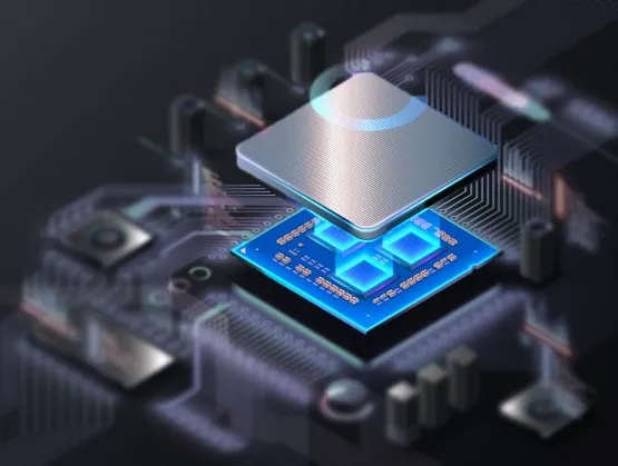
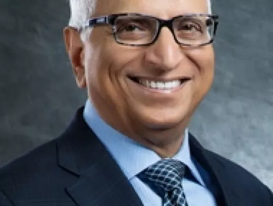
Emerging applications powered by 5G and artificial intelligence (AI) are expected to be a boon to the semiconductor industry, but only once chipmakers overcome a key challenge: Architecting chips that meet the exacting performance, power consumption, size and cost requirements of devices for mid- to high-end applications. One technology – heterogeneous integration – promises to meet these demands and help drive future leaps in semiconductor innovation in the post-Moore era. To help the industry better grasp the technology challenges and business opportunities associated with deploying highly integrated chip and packaging technologies, SEMI and AI on Chip Taiwan Alliance recently gathered industry leaders from organizations including ASE, Unimicron, Dialog Semiconductor, Cadence and AITA to discuss technology trends and the vital importance of building a cross-industry exchange platform to advance next-generation manufacturing processes critical to heterogeneous integration. Following are key takeaways from the forum, Heterogeneous Integration Enables 5G and AI. Overcoming Heterogeneous Integration Technology Challenges Key to Advances in Taiwan High-End Semiconductor Manufacturing The introduction of the Heterogeneous Integration Roadmap (HIR) by the International Technology Roadmap for Semiconductors team in 2016 was an important first step, Dr. C.P. Hung, Vice President of ASE Group, noted in his opening remarks. The HIR is designed to stimulate pre-competitive collaboration to advance heterogeneous integration technology development and accelerate electronics innovation. The roadmap provides a long-term vision for the electronics industry, identifying future technology requirements and potential solutions. Today, the HIR working group focuses on high-performance computing (HPC), 5G and other leading-edge technologies.Dr. Hung predicted that heterogenous integration will reshape traditional collaborations between the semiconductor ecosystem and supply chain in order to clear I/O bottlenecks that hamstring high-performance applications. The retooled industry connections will also need to enable high I/O pin counts, ultra-thin devices, and high-frequency signal shields. In an important step forward, the chip industry today is developing a platform that enhances wafer-level advanced packaging services and deepens cooperation with Oversea Assembly and Testing (OSAT) and substrate supply chain partners. Overcoming the current limits of IC substrates – the connection between IC chips the PCB – is one key for heterogeneous integration technology to flourish, said Dr. Yu-Hua Chen, Vice President, Carrier SBU, RD Division of Unimicron. He noted that the industry must tackle limits to PCB thickness, substrate density, fine pitch and automation to meet the needs of high-end packaging customers. Another barrier the industry must be surmounted is to make the currently inscrutable confidentiality requirements for patents of foreign materials – key to improving chip yields – easier to access and understand for substrate engineers. Chen said partnerships across the entire industry will be necessary to break through this and other technology breakthroughs. Supply Chain and Cross-Border Ecosystem to Strengthen Partnerships for Further DevelopmentTaiwan has long invested heavily in advancing semiconductor manufacturing and application engineering technologies to become a top global chipmaking hub and, in the process, has been behind significant leaps in optimizing chip functionality, said Leroy Liu, General Manager, Asia Headquarters, of Dialog Semiconductor (Germany). With its semiconductor manufacturing prowess, Taiwan can also play a central role in maturing advanced heterogeneous integration packaging technology while managing development costs by partnering with its international supply chain community to overcome technical challenges more effectively, Liu said. The region can also help forge partnerships, even among competitors, to build the ecosystem essential for heterogeneous integration technology to shine.EDA tools will be critical in understanding and resolving heterogeneous integration technical issues since IC substrate, packaging and chip design all pose interdisciplinary engineering challenges, said Julian Sun, Product Marketing Director at Cadence. To help the industry navigate these challenges, Cadence has launched intelligent system design products – solutions that address a wide range of design problems with semiconductor nanometers, micrometers on packaging and testing, and PCB level micro/millimeters to Pin/Pitch, I/O models, and thermals and electricity. By supporting various technical designs, Cadence helps customers shorten the design cycle to strengthen design quality and reduce costs.Sun also pointed to the vital importance of overcoming the significant challenge of designing silicon interposers for heterogeneous integration. Today’s EDA tools are capable of optimizing the design of complex structures including 5GAiP and HBM and are instrumental in aiding Taiwan’s semiconductor ecosystem players to quickly adapt to shifts in the evolving heterogeneous integration market.Heterogeneous Integration Enables 5G and AI speakers (L-R): Julian Sun, Product Marketing Director at Cadence, Dr. Yu-Hua Chen, Vice President, Carrier SBU, RD Division of Unimicron, Dr. C.P. Hung, Vice President of ASE Group, Leroy Liu, General Manager, Asia Headquarters, of Dialog Semiconductor (Germany), Dr. Shih-Chieh Chang, AITA Executive Secretary Designing AI chips is particularly difficult as semiconductor makers struggle with high costs and low yields, said Dr. Shih-Chieh Chang, AITA’s Executive Secretary. That’s why the chip industry now uses FPGAs for small-volume production of AI chips, which makes it easier to improve manufacturing yield through redundant design. For its part, AITA has formed a special interest group (SIG) to help form connections among the chip industry, academia and research institutes. The association’s goal is to build a platform for mass production of AI chips.To get involved in SEMI Taiwan Heterogeneous Integration related events, please contact Ula Huang, outreach senior specialist, at [email protected] Fang is a coordinator and Ashley Huang is a specialist in marketing and public relations at SEMI Taiwan.
Read More
Post-Conference Report: SEMI Heterogeneous Integration SummitDemand for high-performance computing (HPC) chips is exploding. These super-speedy chips are critical for data centers and cloud computing infrastructures to support new performance-hungry technologies such as artificial intelligence (AI) and 5G. The challenge is for the devices and their multi-core architectures to couple high bandwidth density with low latency and high energy efficiency. Heterogenous integration offers a potential answer as an advanced packaging technology designed to meet these skyrocketing performance demands on HPC chips and open the door to a whole new world of 3D integrated circuits (ICs).So important are 3D ICs that Intel and TSMC representatives speaking at the recent Heterogeneous Integration Summit hosted by SEMI Taiwan in Taipei declared that the packaging technology will all but dictate the future of the industry. All told, 12 speakers from government, academia and a broad range of leading international companies from sectors including advanced packaging, design, manufacturing, silicon photonics, equipment and materials shared forward-looking strategies, the latest technologies and potential heterogeneous integration market opportunities. Koushik Banerjee, vice president, TMG, Assembly, and Test Technology Integration, at Intel pointed out that using heterogeneous integration for a single SiP (system-in-package) will deliver what the industry has long wanted by enabling multiple process nodes, more diverse silicon IP (intellectual property) and chip functionality, and chips that pair low energy with high frequency. Intel plans to announce its first Forveros 3D packaging product combining a 10nm HPC chiplet with a low-energy 22nm base die and stacked with memory on top. When asked about the future of advanced packaging technology, Banerjee said it will be very much about the combination of Foveros and its very own Embedded Multi-Die Interconnect Bridge (EMIB).For its part, TSMC, will continue to upgrade its CoWoS (Chip-on-Wafer-on-Substrate), InFO (Integrated Fan-out) and other 2.5D IC production solutions while developing 3D chip stacking technology such as SoIC and WoW (wafer-on-wafer). TSMC is ushering in a new age of 3D IC packaging, said Marvin Liao, Vice President, Backend Technology and Service Division, at TSMC. The company’s SoIC is based on Chip-on-Wafer concept, with the flexibility to support one-to-many or different process nodes, whereas its WoW integrates two wafers with solid yields that could be used for products of the same size or manufactured with mature process technology.Speakers also included representatives from ATOTECH, Lam Research, SPIL, Sigurd, Cadence, Grand Process Technology, ITRI (Industrial Technology Research Institute), Industrial Development Bureau, and Lee San-Liang, Distinguished Professor, Department of Electronic and Computer Engineering at National Taiwan University of Science and Technology all shared their perspectives on equipment, materials, and testing and how different industry value chains might contribute to the development of heterogeneous integration technology.Expected to be a key driver of the next wave of semiconductors, heterogeneous integration and related technologies – including 3D IC, FOWLP (Fan-out wafer-level packaging) / FOPLP (Fan-out panel-level packaging), silicon photonics, Micro LED, compound semiconductor, automated optical inspection and SLT (system level testing) – will be a key focus at SEMICON Taiwan 2019, September 18 to 20 in Taipei. The Heterogeneous Integration Innovation Zone – along with featured international programs such as SiP Global Summit, Strategic Materials Conference, the Smart Data Summit and the Smart Automotive Summit – will gather key industry players to reveal the latest technology breakthroughs and market trends.Emmy Yi is a senior marketing specialist at SEMI Taiwan.
Read More
New SEMI Taiwan Testing Committee to strengthen the last line of defense to ensure the reliability of advanced semiconductor applications.Mobile, high-performance computing (HPC), automotive, and IoT – the four future growth drivers of semiconductor industry, plus the additional boost from artificial intelligence (AI) and 5G – will spur exponential demand for multi-function and high-performance chips. Today, a 3D IC semiconductor structure is beginning to integrate multiple chips to extend functionality and performance, making heterogeneous integration an irreversible trend. As the number of chips integrated in a single package increases, the structural complexity also rises. Not only will this make identifying chip defects harder, but the compatibility and interconnection between components will also introduce uncertainties that can undermine the reliability of the final ICs. Add to these challenges the need for tight cost control and a faster time to market, and it’s clear that semiconductor testing requires disruptive, innovative change. Traditional final-product testing focusing on finished components is now giving way to wafer- and system-level testing.In addition, the traditional notion of design for testing, an approach that enhances testing controllability and observability, is now coupled with the imperative to test for design, which emphasizes drawing analytics insights from collected test data to help reduce design errors and shorten development cycles. Going forward, the relationship among design, manufacturing, packaging, and testing will no longer be un-directional. Instead, it will be a cycle of continuous improvement.This paradigm shift in semiconductor testing, however, will also create a need for new industry standards and regulations, elevate visibility and security levels for shared data, require the optimization of testing time and costs, and lead to a shortage of testing professionals. Solving all these issues will require a joint effort by the industry and academia. "With leading technologies and $4.7 billion in market value, Taiwan still holds the top spot in global semiconductor testing market," said Terry Tsao, President of SEMI Taiwan. "When testing extends beyond the manufacturing process, it can play a critical role in ensuring quality throughout the entire life cycle from design and manufacturing to system integration while maintaining effective controls on development costs and schedules. Taiwan's semiconductor industry is in dire need of a common testing platform to enable the cross-disciplinary collaboration necessary for technical breakthroughs."The SEMI Taiwan Testing Committee was formed to meet that need, gathering testing experts and academics from MediaTek, Intel, NXP Semiconductors, TSMC, UMC, ASE Technology, SPIL, KYEC, Teradyne, Advantest, FormFactor, MJC, Synopsys, Cadence, Mentor, and National Tsing Hua University to collaborate in building a complete testing ecosystem. The committee addresses common technical challenges faced by the industry and cultivates next-generation testing professionals to enable Taiwan to maintain its global leadership in semiconductor testing.The SEMI Taiwan Testing Platform spans communities, expositions, programs, events, networking, business matching, advocacy, and market and technology insights. For more information about the SEMI Taiwan Testing platform, please contact Elaine Lee ([email protected]) or Ana Li ([email protected]). Emmy Yi is a marketing specialist at SEMI Taiwan.
Read More
SEMI’s mantra is: Connect, Collaborate, Innovate. This mantra has delivered industry-enabling value to our members since SEMI’s beginnings in 1970. It has been essential for SEMI members to grow and prosper locally, while being synchronized globally. As the electronics manufacturing business has become more complex and interdependent, SEMI’s mantra has increasingly been applied across the full span of electronics manufacturing.With the IC industry now worth over $400 billion in annual revenue, developing a single new chip can cost hundreds of millions of dollars. Consequently, industry players now connect, collaborate, and innovate in new, but more often, deeper ways. This is especially true with IC design – what’s possible in chip design is only possible if the manufacturing processes can be developed as projected. It makes sense, as complexity grows and the stakes get higher, that design and manufacturing are closely linked and apply the SEMI mantra together. Where Electronics Begin“Where Electronics Begin” is the tagline of the Electronics System Design Alliance, or the ESD Alliance. It aptly distills the fact that all IC manufacturing begins with design – and the design ecosystem. This week, SEMI announced it reached an agreement with the ESD Alliance to join SEMI as a SEMI Strategic Association Partner. The ESD Alliance will become part of the SEMI organization in 2018. With the ESD Alliance and its community joining SEMI, its membership will complete the full electronics design and manufacturing span.This is a momentous step forward. The ESD Alliance’s ecosystem is vital and thriving and includes the world’s leading EDA and IP companies. Within the ESD Alliance community, Aart de Geus (Synopsys), Wally Rhines (Mentor, a Siemens Company), Simon Segars (Arm), and Lip-Bu Tan (Cadence), among others, are already familiar figures, having brought their thought leadership to SEMI platforms in the past. Now they, and the rest of the ESD Alliance members, will be able to more directly work with semiconductor equipment manufacturers, devices makers, and the rest of SEMI’s membership.At events like SEMICON China, which recently concluded in March and attracted over 90,000 attendees, SEMI and the ESD Alliance members will be able to efficiently connect and engage the supply chain players and find new areas for collaboration. As SEMI’s membership looks out towards new applications and systems opportunities, having both ecosystems together will find possibilities faster and innovate approaches more practically. The ESD Alliance will maintain its distinct community identity and governance while having access to, and the ability to augment, SEMI’s global platforms including seven regional offices, programs and expositions (including SEMICONs), advocacy (including trade, tax, talent, and technology), industry research and statistics, and other SEMI Strategic Association Partner and technology communities.SEMI will gain direct access to the electronics design ecosystems to provide a deeper and wider value – to its combined membership – with SEMI’s mantra. SEMI and its more than 2,000 corporate members and more than 1.2 million stakeholders look forward to connecting, collaborating, and innovating with the ESD Alliance and its members. SEMI’s global reach and wide span of membership with ESD Alliance’s deep expertise in design and IP is truly the best of both worlds for all stakeholders.Connect: Design ManufacturingSEMI’s members have been reaching into the electronics design ecosystem and the ESD Alliance members have been reaching into SEMI’s ecosystem to optimize design and manufacturing process for lowest cost and highest yield. This week’s announcement is a step forward to directly and more intimately connect electronics design and manufacturing for the supply chain to work more closely together in full synchronization. Collaborate: From Beginning to End in Electronics ApplicationsWith the ESD Alliance joining SEMI as a Strategic Association Partner, SEMI members can better collaborate across the full supply chain. Gone are the days when it was enough to collaborate only with one’s direct customer. Today, for example, components and c-subs suppliers frequently collaborate not just with their OEM equipment manufacturer customers, but with device manufacturers – and even system integrators. To be successful, companies are striving for connection to their customers’ customers.The ESD Alliance, with its design ecosystem and linkage to the fabless community, will join three existing SEMI Strategic Association Partners: Fab Owners Alliance (FOA), MEMS Sensors Industry Group (MSIG), and FlexTech (the association representing the flexible hybrid electronics ecosystem). These relationships now cover the entire span of electronics manufacturing.To provide focused collaboration across the full supply chain, SEMI has developed five vertical application platforms: IoT, Smart Manufacturing, Smart Transportation, Smart MedTech, and Smart Data. These have been chosen because of unique and pressing needs to synchronize the supply chain and to engage and develop solutions collectively.Innovate: Faster FutureWith the confluence of emerging digital disruptions and new demand drivers, forecasts suggest the IC industry could grow to over $1 trillion in annual revenue by 2030. To deliver this growth, the supply chain must efficiently innovate together. SEMI’s value proposition is to speed the time to better business results for its members across the global electronics (design and) manufacturing supply chain. The addition of the ESD Alliance as a Strategic Association Partner is a key contributor to deliver this value proposition for the industry to grow and prosper now and in the future.
Read More