downloadGroupGroupnoun_press release_995423_000000 copyGroupnoun_Feed_96767_000000Group 19noun_pictures_1817522_000000Member company iconResource item iconStore item iconGroup 19Group 19noun_Photo_2085192_000000 Copynoun_presentation_2096081_000000Group 19Group Copy 7noun_webinar_692730_000000Path
Skip to main content
Default Banner Image

printed electronics

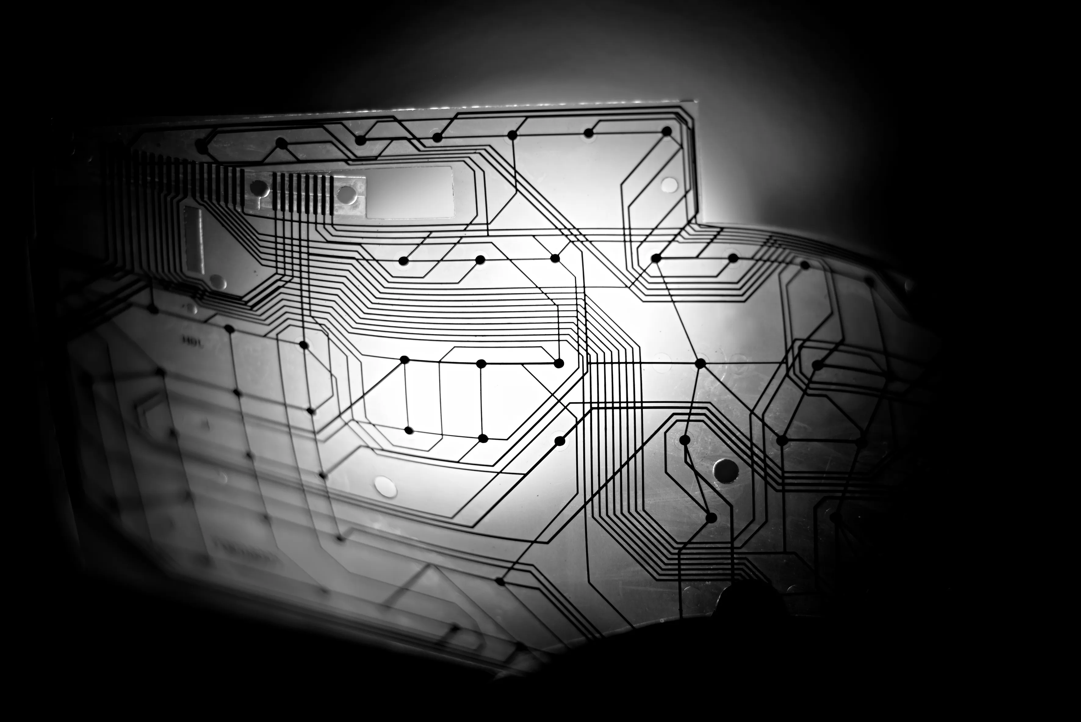
Presentations at this year’s FLEX Conference illustrated the ongoing development of manufacturing tools and processes, materials, and test and reliability evaluation techniques for the growing field of hybrid electronics, which includes printed electronics and flexible hybrid electronics (FHE). Additionally, the field includes the use of additive manufacturing processes for electronics packaging and system assembly, from die attach to flexible printed circuits.Hosted by FlexTech, a SEMI Strategic Technology Community, the conference provides an opportunity for the device making supply chain to connect to R D, design and manufacturing innovations. A review of some of the key developments highlighted in FLEX presentations follows.Innovations in Flexible Printed CircuitsTokyo-based Elephantech has been focused on using advanced inkjet systems to produce flexible printed circuits. Using additive methods instead of subtractive to produce PCBs can enable reductions in carbon footprint, copper usage and water consumption. In order to achieve these benefits, Elephantech has developed processes for combining inkjet printing of metals and electroless plating. The company synthesizes copper nano particles, which it uses to formulate metal ink. It has implemented artificial intelligence to increase print accuracy, showing the capability of average drop position error of less than 2μm, and depositing 20μm droplets into 40μm grooves and wells (Fig 1).Fig. 1. Elephantech inkjet results showing ~2μm precision and prototypes with 50μm line widthExamples of Elephantech’s use of flexible printed circuit technology include a set of switches for a curved monitor and a pressure sensor with reduced footprint and component count. The company intends to directly compete with larger, rigid PCBs, and is developing a mass-production system with 57,840 nozzles that can process sheet sizes of 500 x 830 mm.Traditional processes for component attach on PCBs include mass reflow ovens, thermal compression bonding, and spot laser reflow. Laserssel has developed laser selective reflow, which promises warpage- and damage-free bonding at increased processing speeds. In addition to improving the productivity of rigid PCB production, the laser selective reflow could also enable in-line processing of roll-to-roll flexible printed circuits, replacing the use of trays for bonding to flexible printed circuits.Scrona, which spun out from ETH Zurich, has developed MEMS-based printheads to improve electrohydrodynamic (EHD) printing. By using an electric field to pull droplets out of the print nozzle, EHD can enable much higher print resolution (sub-micron, compared to tens of microns), and enable the use of higher viscosity inks than would be possible with traditional inkjet heads. While EHD has been under development for some time, its application has been limited by crosstalk, in which the electric fields of adjacent nozzles interact with each other, and the requirement for the nozzle to be within tens of microns from the substrate to enable high print accuracy.Scrona’s MEMS-based nozzles address these EHD problems by shielding adjacent nozzles to prevent crosstalk and by creating a uniform electric acceleration field, which increases print distance to the order of a millimeter. The company has used its system to print a variety of inks on different substrates, as well as conformal printing on 3D surfaces (Fig. 2).Fig. 2. Example of printing silver wires across a polished glass edge; line pitch 25μm, glass thickness 1mmThe Rochester Institute of Technology (RIT) has been developing an additive technique called liquid metal droplet jetting, which can deposit metal traces functionally equivalent to solid wires. The process uses metal wire as a feedstock, which is a fraction of the cost of nanoparticle metals. While tin, zinc, and aluminum have been used, silver and copper are still under development. The wire is melted in a micro-crucible, which feeds a nozzle; metal droplets are then jetted on demand in an argon environment to prevent oxidation (Fig. 3, l). Upon hitting the substrate, the drops solidify into metal traces equivalent to solid wire, quickly enough to avoid melting flexible films, and without curing or drying.Several methods have been explored to eject the jets from the nozzle, including magnetohydrodynamic using electromagnetic pulses, piezo-actuated pistons, and pneumatic jetting using compressed gas (Fig. 3, r). These techniques range from high-jetting-frequency and high-cost to simple and low-cost but low-frequency. Higher frequency enables overlap of droplets, increasing conductivity, and reduced processing time.Fig. 3. Concept of liquid metal droplet jetting (l); pneumatic droplet ejection approach (r)In addition to ongoing development of deposition tools and processes, the material set for additively printed electronics continues to expand. Iris Light Technologies, which spun out of Argonne National Lab and Northwestern University, is developing photonic inks for wafer-scale production of active devices including photodetectors, LEDs, and lasers. The semiconductor-based ink can be deposited via aerosol jet onto silicon wafers. Iris Light is focused on 2D semiconductors, specifically black phosphorous, which has a wider spectral coverage than graphene, is tunable in emission and absorption, and has high mobility.An example of the broadening of the additive manufacturing supply chain, Kraetonics has developed software for creating slices to be used in designing 3D-printed structures and elements. The software enables manufacturing 3D volumetric circuits with reduced size, weight, and power compared to 2D PCBs. The process involves 3D printing of hybrid mechanical-electrical assemblies such as circuits and antennas.Innovations in Test and ReliabilityAn area of active interest in the hybrid electronics community is that of test and reliability. American Semiconductor, a developer of flexible circuitry, and Bayflex, a value-added partner of Japanese equipment company Yuasa, are conducting a project on dynamic harsh environmental FHE reliability testing. The goal is to identify root causes of FHE material and system failures.The companies are developing extended temperature and humidity tests to determine FHE system lifetimes and identify causes of failures from physically deforming FHE materials and systems in harsh temperature and humidity environments. Materials under consideration for testing include:Copper on polyimide substrate with a small outline package IC and surface-mounted componentsNobleflexTM, a multilayer substrate with gold on polyimide in development for medical devicesSilver on PET substrate, with small outline package IC.The team is soliciting other test devices and is planning to coordinate with ongoing development of FHE test standards coordinated by SEMI.Henkel reported on an investigation of accelerated temperature cycling test methods, in which the company applied different combinations of temperature range, stress, and frequency of mechanical force in an effort to reduce cycle time for testing component attach reliability. The study was able to achieve similar failure modes using an accelerated test method in the case of a bonding position shift in which cracking of the die attach film was the failure mode (Fig. 4, approach 4). The study found the greatest acceleration in the case of reduced thermal shock cycles (Fig. 4, approach 1).Fig. 4. Approaches evaluated for accelerated testing of component attach.Engineering consulting firm Exponent presented the results of a study on mechanical testing for characterizing fatigue performance of flexible electronics, conducted with continuous monitoring of fatigue for 6-pin flexible flat cables from seven different vendors. Exponent found that continuous monitoring during bending fatigue testing provided greater resolution in test results including detection of intermittent failure in each sample. The study also found that strain amplitude was a critical factor for determining fatigue life, and that flat flexible cables with larger pitches showed improved fatigue performance.About SEMI FlexTechFlexTech, a SEMI Strategic Technology Community, promotes the growth, profitability and success of the flexible hybrid electronics industry by developing educational forums, directing research, and promoting technology innovation.SEMI FlexTech members benefit from speaking and business networking opportunities, introductions to key industry players, research reports, technical funding, access to end users and industry advocacy at FLEX Conferences.Gity Samadi is Director of SEMI research and development funding programs and SEMI FlexTech and SEMI Nano-Bio Materials Consortium (NBMC). Paul Semenza is an advisor to SEMI on special projects. He was previously with NextFlex, the Flexible Hybrid Electronics Manufacturing Innovation Institute.
Read More
For the first time in its 20-year history, the FLEX Conference dedicated an entire session to the important and timely twin topics of environmental sustainability and power consumption of electronic devices. The event planning committee recognized the urgent need to increase the awareness of how technology and electronics devices can help reduce greenhouse gas emissions (GGE) overall and meet aggressive targets to curb the impacts of climate change. Dr. Christine Ho, CEO of Imprint Energy, delivered the keynote for the session, focusing on the need for powering billions of sensors that will be deployed annually, and their role in reducing fossil fuel emissions through becoming aware of issues, monitoring our resources over time, and intervening early and often to combat waste in multiple sectors and industry. Quoting extensively from the organization Exponential Roadmap Initiative (ERI), Ho noted that “the digital sector has the potential to directly reduce fossil fuel emissions 15% by 2030 and indirectly support a further reduction of 35% by influencing consumer and business decisions and systems transformation.” The initiative’s playbook for reaching net zero carbon emissions by 2050 and limiting global warming to 1.5° Celsius outlines how the digital sector can help remove 13 of the 27 gigatons (GT) of CO2 needed to reach this goal. Ho stated that the rapidly emerging Internet of Things (IoT), devices, software systems, and data insights are the backbone of this digital transformation. The IoT's vast network of sensors can transform multiple sectors, such as the logistics industry, which on an annual basis moves and ships more than 10 billion tons of products worldwide by ships, airplanes, long haul trucks, and train - contributing 17% of GGE and more than 4 gigatons of CO2 annually. Always-connected IoT sensors used by the logistics industry can reduce waste and damage in the supply chain, which is especially problematic for temperature-sensitive and damage prone pharmaceutical and food products, mitigating the need for producing high volumes of buffer inventory to replace damaged goods Noting that the attendees of 20 Years of FLEX Conferences were a big part of the current advancements of low-cost printed, active, shipping tags, Ho said that Imprint Energy’s flexible and thin, Zinc based batteries are ideal for IoT devices, since they boast a significantly smaller carbon footprint than Lithium-Ion (Li-ion) batteries. Imprint Energy is working with systems designers and integrators to design the battery as an integral part of the device package and use low-power strategies to extend device lifetimes. Imprint recommends co-locating battery printing alongside the device integration to further minimize shipping and logistics. When manufactured separately, Imprint’s small footprint, low-operating temperature process line (less than 80°C) provides significant carbon footprint advantages over other technologies. Ho challenged the attendees, saying “we all need to participate in protecting our earth. We need to eliminate waste and contribute to reducing half of our current greenhouse gas emissions by 2030, and we can do that by deploying a global digital skin with more than 100 billion IoT devices in 2030 and up to 1 trillion by 2050. We can minimize the device carbon footprint and maximize its longevity by considering the power capability, as well as design for re-use and re-cycling of the critical materials.” Following Dr. Ho’s presentation, FLEX kicked off a spirited panel discussion with experts from PowerRox, ITN Energy Systems, Birla Carbon, and Auburn University and chaired by Bob Praino and Eric Forsythe, from Chasm Advanced Materials and the Army Research Labs, respectively. The speakers summarized their on-demand presentations and looked at what is being done today to recycle Lithium-Ion batteries, how IoT devices are currently being powered, and drew comparisons between the early days of the Internet and development of the IoT. The speakers generally agreed that the power requirements of wireless cellular and Blue-tooth devices were still too high and run times too short. FLEX 2021 was a virtual event in the 2021 SEMI Technology Series. It was organized by SEMI FlexTech, SEMI NBMC, and NextFlex. Major sponsors included E Ink and Novacentrix. The event covered technical developments in flexible, printed and hybrid electronics, featuring more than 100 presentations and networking opportunities. Technical proceedings are available until March 26 at http://flex.semi.org. Heidi Hoffman is senior director in Corporate Marketing at SEMI.
Read More
Is your company working on the next big thing in flexible, hybrid and printed electronics – a breakthrough or innovation that will make the world safer, healthier or more productive for years to come? If so, we want to hear from you.You’re invited to deliver a technical presentation at virtual FLEX 2021, February 22-26, 2021. The call for abstracts is now open! Celebrating its 20th year, the online event will gather executives, product managers, business development professionals, and engineering directors as well as leading industry analysts and media for the latest developments, trends and innovations in flexible hybrid electronics (FHE). More than 400 companies, universities, R D labs, and government agencies from around the world have participated in FLEX conferences.Technical presentations should focus on the conference theme, 20 Years of Driving Innovation to Make the World Safer, covering flexible hybrid or printed electronics products, equipment, processes, materials, and the applications they enable. FLEX 2021 also takes aim at the future of the planet, so presentations on global sustainability in areas such as impacts, strategies, tactics, successes and progress area also a great fit. To submit your abstract, please complete the online form: Upload your abstract (100-300 words) describing the topic of your presentation and how it applies to the flexible, hybrid, and printed electronics products. Preference is given to original research and advancements in process and materials as they relate to end users. We also invite students from research universities to submit posters describing their work and results for the popular FLEX Poster Competition. As in the past, a panel of industry and academic experts will evaluate the posters and recognize the top three students and their work. Here are key deadlines and dates for industry experts and students to keep in mind: September 30, 2020 – Submit your abstract. October 31, 2020 – We’ll notify you whether your presentation has been accepted by this date. November 15, 2020 – Sign a Speaker Agreement and provide a bio and headshot. February 1, 2021 – Send us an electronic copy of your presentation. We’re looking for presentations in these topic areas: Flexible Hybrid Electronics Systems Materials Processing Sustainability and Power MEMS and Sensors Applications Presentations should include the following: Why the technology presented matters and to whom Practical recommendations for addressing commercialization issues or applications. This includes providing innovative technological or market solutions driven by a use case, the integration challenges you faced, and the system-level architecture decisions you made. Descriptions of how you overcame each challenge Ideas for what as an industry we should be working on and what are you working on to demonstrate sustainability For a full rundown on topics and other information, please visit the FLEX 2021 Call for Papers web page.Michelle Fabiano is a program and event manager for SEMI Americas.
Read More
Since 2015, FlexTech has funded three projects with ITN Energy Systems, based in Littleton, Colorado. The projects all draw on a unique concept of using thin, flexible ceramic sheets as both a substrate for functional devices and as an integral part of the hermetic packaging to support paper-thin FHE products. Each program was increasingly sophisticated, enabling a larger variety of functions to be integrated into a common package. Independent functions such as energy storage, energy harvesting, or printed microelectronic circuits are deposited on their own ceramic substrate and the layers vertically stacked and interconnected into a monolithic structure that combines several functions in the smallest possible package volume.The ITN projects provide excellent examples of the power of collaborative research and development to help de-risk investments in next-generation electronics. All the projects were conducted with technical contributions from small and large businesses as well as university partners. The programs were funded by the U.S. Army Research Laboratories (ARL), directed by industry leaders and managed by SEMI FlexTech with the focus on utilizing the advantages of flexible hybrid and printed electronics (FHE) to create lighter-weight, lower-power, more conformable electronics than available commercially today. Markets ready to take advantage of FHE developments include healthcare, aerospace, mobility, consumer electronics, industrial electronics.ITN was founded in 1995 to focus on researching and developing technologies related to aerospace, energy and the environment for defense and commercial marketplaces. Its business model employs collaborative R D projects to explore, develop and validate promising next-generation clean energy technologies with an emphasis on tackling the manufacturing challenges that enable low-cost, high-volume production of thin-film devices on flexible substrates. Those technologies that meet the technical and business requirements of the market are commercialized via focused, spin-out companies with five such spin-outs formed so far. The work on ultra-thin batteries needed by the SEMI FlexTech community readily slid into their portfolio of projects.Project 1 – New Solid-State Lithium BatteryThe first project kicked off in 2016, with ENrG, and successfully supported the development and validation of novel Solid-State Lithium Battery (SSLB) products with total packaged thickness ranging from 50-250 microns. The SSLB proved to have substantial advantages in form factor and performance when compared with both commercial-off-the-shelf batteries and emerging technologies. For example, the SSLB provided more than double the operating time in a substantially smaller package in powering an audio device supplied by SEMI FlexTech partner companies.By avoiding the use of liquid electrolytes, the ITN SSLB also eliminates flammability issues while still allowing the benefits of lithium-based battery chemistry. The SSLB boasted many attributes attractive to the FlexTech community, including: Ultra-thin form factor, i.e. 250 microns thick, mAh class packaged batteries High volumetric energy density, i.e. baseline products with ~500 Wh/l and a roadmap to 1,000Wh/l The ability to support high current pulsing, i.e. current pulses at 4-10C rates, in support of demanding FHE duty cycles High temperature compatibility with solder reflow and other FHE integration schemes Rechargeability with high capacity retention at 1,000 cycles This new SSLB has formed the foundation of subsequent projects and commercialization efforts.Project 2 – Adding Energy Harvesting Based Recharging Capability The second SEMI FlexTech-funded project proposed a novel self-recharging battery with the addition of Lucintech’s cadmium telluride (CdTe) photovoltaics (PV), which was also deposited on thin yttria stabilized zirconia (YSZ) substrates. Because the CdTe supports a superstrate configuration, the SSLB can function as the back sheet for the PV package, thereby dramatically decreasing overall package thickness. The resulting flexible integrated power pack provided up to 0.25 Wh of energy storage and ~0.2 W of PV generating capacity in a total package less than 250 microns.As part of that effort, the ITN Team identified an effective power-management circuit that was ultimately compatible with die thinning and form factors very attractive to FHE. Consequently, the PV and SSLB were interconnected into a common power bus that enabled FHE to be operated with either the PV, SSLB or some combination of the two.ITN is seeing great interest in this product and both developing a version with substantially higher capacities than the project entertained for a UAV platform while ramping to low volume with support from NextFlex, a member of the Manufacturing USA network, and formed in 2015 through a cooperative agreement between the U.S. Department of Defense (DoD) and FlexTech Alliance.Monolithic integration of function layers atop of SSLB for high performance microelectronics device Project 3 – Integration with Processing and Sensor SystemsThe third FlexTech-funded project builds further on that foundation. In this project, the ITN Team is maturing the technologies to create a battery with an integrated processing and sensor system, nicknamed BiPASS. In addition to SSLB layers, the BiPASS package integrates printed circuits on YSZ employing high-performance, silicon- based bare die micro-electronics and/or thin film sensors into the common packaging. Mock-up of the charge control circuit on SSLB The initial demonstration integrates a commercial lithium battery charge control circuit within the SSLB packaging to create a monolithically integrated power module. There have also been promising developments of the University of Rhode Island’s metal oxide (MOx)-based thin film gas sensors that have dramatically increased sensitivity when deposited on thin YSZ. The resultant sensor achieves ppb detection of trace explosives gases that can be powered by SSLB. Along the way, ITN’s partners Molex and SunRay Scientific matured several aspects of FHE circuit printing and integration on both PET and YSZ, including new materials and processes for conductive traces, and bare die attachment with fine features. The project is in its final stages and the ITN Team now has a promising roadmap to integrate power, microelectronics, and thin film sensors/sensor systems into a single paper-thin package.Commercial Scale-Up StrategySince the initial demonstrations were completed, ITN has been actively maturing a commercial scale-up strategy based on significant market-pull and interest from several companies. A new venture to commercialize this next generation SSLB is in process. As part of those discussions, ITN is in active discussions with potential strategic partners to support the transition to high-volume production to access additional markets, many of which are cost-sensitive and need a higher degree of production maturity.In the meantime, ITN’s limited volume SSLB production line is already supporting medical device customers. In addition, a baseline SSLB (~2.5 mAh capacity) has been developed and tested in several new applications, including wearables, sensors and smart labels.“Based on the acceptance of these project in the market, I believe all three projects have provided significant value to the SEMI FlexTech community,” noted Brian Berland, Chief Technology Officer at ITN. “In addition, the connections and visibility we have gained within the industry by partnering with SEMI FlexTech have been invaluable. We are excited to continue this journey with new and additional projects. In the meantime, we are hopeful that our ongoing discussions with investment partners will support our commercializing of these components.”For more information visit www.flextech.org. SEMI FlexTech is currently (from 6/10/2020 – 7/17/2020) accepting white papers for new technology development projects. Read more at www.flextech.org.About the AuthorDr. Gity Samadi is the SEMI FlexTech Program Manager. Gity is responsible for the flexible hybrid electronics R D consortium activities including project awards and management, Technical Advisory Council management, and webinar/industry event planning for the building and fostering of this dynamic innovative community.
Read More
Most of today’s blockbuster MEMS products – from pressure sensors and resonators to accelerometers and microphones – originated from academic research, a trend that Alissa M. Fitzgerald, Founder Managing Member, A.M. Fitzgerald Associates, expects to continue. While many of these potentially game-changing new technologies will require many more years of intensive development and up to $100 million in investment to reach full commercialization, Fitzgerald sees their potential for generating new waves of activity and opportunity in the MEMS and sensors industry.SEMI’s Maria Vetrano caught up with Fitzgerald to preview her October 23 presentation, Emerging MEMS Sensors Technologies to Watch as We Enter a New Decade, at MEMS Sensors Executive Congress, October 22-24, 2019, at the Coronado Island Marriott Resort Spa in Coronado, California.Join us at MEMS Sensors Executive Congress (MSEC) to meet Alissa Fitzgerald and other industry influencers driving innovation in the MEMS and sensors industry. Register now to connect with her at MSEC or visit her on LinkedIn.SEMI: What are your top three emerging MEMS and sensors technologies with the greatest promise?Fitzgerald: Let’s start by defining emerging. In researching this topic for MSEC, I reviewed a year’s worth of academic papers to search for compelling technologies that will emerge five to 10 years from now. While these applications are not yet commercially ready, they bear a distinct presence in academic literature, and some have even reached the proof-of-concept phase. They all have the potential to advance user functionality derived from MEMS and sensors in very meaningful ways.Next-Generation MicromirrorsI’ve noticed renewed interest in micromirrors, driven by interest in LiDAR for autonomous vehicles, in fiberoptic networking, and in VR/AR glasses and headsets as well.Newer generations of micromirrors will use piezoelectric films to enhance optical performance. Piezoelectric actuation can pivot the mirror to a much larger angle than older-generation electrostatically actuated micromirrors. This is important for wider-angle scanning for LiDAR – as well as for other applications – as it enables the creation of a larger picture image.Piezoelectric films can also be used to change the shape of the mirror surface to enable a variable-focus mirror. This is useful on two fronts: It supports depth-of-field adjustments and it alleviates the need for extreme precision in packaging of optical devices, improving both cost and yield.Event-driven sensors/zero-power/ultra-low power sensorsSensors that draw no power, or that draw just small amounts, by activating only upon a triggering stimulus, are enormously exciting. Their extremely low power consumption addresses one of the most significant obstacles to creating large-area sensor networks: the problem of too-frequent battery changes.In addition, while most sensor nodes today broadcast a large stream of data back to the mother ship by radio, these event-driven or zero-power sensors consume only a small amount of power because they activate the radio only to transmit essential data.Resolving the power-consumption problem with sensors will allow deployment of large-area sensor networks in remote or inaccessible locations, highly useful for applications such as monitoring infrastructure.Bacterial sensorsSensors that can detect the presence of bacteria, as well as the type, have widespread applicability beyond medical uses. They would be particularly useful in food-safety applications as they can identify particular strains of bacteria, such as E. coli, before the beef leaves the processing plant or the spinach ships from the warehouse. This could offer dramatic improvements in food safety over the Centers for Disease Control (CDC) and U.S. Food and Drug Administration’s (FDA’s) food safety program, which only flags foodborne illness when a cluster of people are seriously ill.Researchers are also designing bacterial sensors for rapid point-of-care (POC) diagnostics to detect, for example, sepsis early, potentially saving lives.SEMI: You’ve said that some future MEMS and sensors will use alternatives to silicon. When might we see MEMS and sensors printed on paper or other flexible materials – and for which applications are they suited?Fitzgerald: We’re seeing an enormous amount of development of sensors made on paper, plastics and even textiles, materials that are readily available, inexpensive and flexible.What’s gating our progress right now is manufacturing infrastructure. At present, researchers are using inkjet printers, 3D printers, etc. to manufacture prototype sensors, but in most cases, they would need to move to roll-to-roll printing to scale up. I think that we’re looking at a decade before we see these sensor technologies reach the mass market.When they do arrive, we’ll see sensors that we can easily affix to any kind of carton, wrapper or packaging used with food or other disposable items. Traceability and status of perishable items in particular will allow consumers to track food from the farm or factory to the warehouse, store and, finally, to the home.Implementing these kinds of sensors would also help the environment. According to the Natural Resources Defense Council, in the United States alone up to 40 percent of our food is wasted annually, in part because we fear it’s gone bad. If consumers feel assured that their food is safe, they will waste less. And wasting less means that we can grow less food to feed the same number of people. We’ll also reduce the volume of food waste that goes to landfills.SEMI: What can the MEMS industry do to promote the use of more environmentally friendly materials in its products?Fitzgerald: Some of this is already underway. More companies in our industry are adopting Restriction of Hazardous Substances (RoHS) standards to get rid of heavy metals, such as lead, cadmium or other hazardous materials, in their electronics.We could also produce disposable sensors on paper or on biodegradable plastics, which would decompose within a few months, and we could use safer metals, such as gold, magnesium or zinc, to reduce hazardous metals’ contamination in landfills. While it’s not feasible to make all sensors biodegradable, the market for such sensors could be massive.As companies (and individuals), we should also work hard to design electronics that consume less power, because this ultimately translates to fewer disposable batteries in landfills.SEMI: What would you like MSEC attendees to take away from your presentation?Fitzgerald: I’d like to make two main points. First, the trend to use other non-silicon materials to make MEMS and sensors is real and inevitable. It’s a matter of when. Anyone building a gas or chemical sensor on silicon should look at how to do it on paper or plastic because there are great future applications incorporating flexible, disposable sensors in packaging of all types. That’s the low-hanging fruit.Second, to support this technology development trend, we must look seriously at manufacturing infrastructure because we will need completely different sets of equipment, environments and consumable materials to manufacture MEMS and sensors on paper or plastic. Sensor manufacturers could prepare for this future expansion by beginning to collaborate today with companies that already produce paper and plastic goods. Alissa Fitzgerald, Ph.D., founded A.M. Fitzgerald Associates, LLC (AMFitzgerald), a MEMS and sensors solutions company, in 2003. She has over 20 years of engineering experience in MEMS design, fabrication and product development.Prior to founding AMFitzgerald, Fitzgerald worked at the Jet Propulsion Laboratory, Orbital Sciences Corporation, Sigpro, and Sensant Corporation, now part of Siemens. She received her bachelor’s and master’s degrees from MIT and her doctorate from Stanford University, in Aeronautics and Astronautics. Fitzgerald has numerous journal publications and holds eight patents. She served on the Governing Council of MEMS Industry Group from 2008-2014 and was inducted into the MIG Hall of Fame in 2013. Fitzgerald serves on the Board of Directors of both Rigetti Computing and the Transducer Research Foundation.For more information, please visit AMFitzgerald.MEMS Sensors Industry Group (MSIG), the industry association representing the global MEMS and sensors supply chain, hosts the annual MEMS Sensors Executive Congress. To learn how MSIG enables professionals in the MEMS and sensors industry to innovate, address common challenges and accelerate business results, visit us today.Maria Vetrano is a PR consultant for MSIG, a SEMI Strategic Association Partner.
Read More
How are flexible electronics impacting the automotive sector? How will medical diagnostics and life sciences be changing with the advent of flexible, conformable electronics? How does space exploration intersect with the continued development of flexible sensors and Internet of Things (IoT) systems? The upcoming 2019FLEX Japan / MEMS SENSORS FORUM in Shinagawa, Tokyo, May 22-23, 2019, will explore these questions and more. The event, the third FLEX Japan, is expected to gather 300 designers, technologists, researchers, analyst and product developers to hear presentations, discuss their approaches, and create connections. The transformation of the automotive industry will receive special attention with speakers from Yole Développement and a deep exploration of the new sensor form factors and capabilities. Professor Shoji Kawahito of Shizuoka University will discuss the impact of image sensors on automotive LIDAR, night vision and monitors for the driver and passengers. Dr. Yoshifumi Sakamoto of IBM Japan will share his views on key trends in smart transportation and what they mean for the supply chain. Beck Oh, president and CEO of PNI Sensor, will share how parking sensors are transforming our driving – and parking – experience. Hideo Fukunaga, project manager for Velodyne LiDAR, will discuss his work using LIDAR, often seen as the most promising and the most difficult and expensive component of autonomous driving. Jerome Joimel, CTO of ISORG, will discuss integration of organic image sensor behind display.Medical and home electronics devices are moving out of their boxes and hospitals, and flexible electronics, new sensor designs and new power options are playing a major role in that transformation. Jenax, Kobe University, Toyo University, Osaka University, and Daiwa House are just some of the presenters in this area. Researchers are steadily overcoming key technology hurdles, such as electronic interconnects between soft and rigid surfaces, and energy harvesting techniques for no-power devices, as well as ultra-thin RF components, and advanced microfluidic systems. Space, the final frontier, will be the backdrop for the general keynote talk of Mayya Mayyappan, chief scientist for exploration technology at NASA’s Ames Research Center. His team is investigating new printed and flexible sensors and electronics that can be printed in zero-gravity and how these devices will enable IoT.The only event in Japan focused on flexible and printed electronics, with special focus on the complementary areas of sensors and MEMS, 2019FLEX Japan / MEMS SENSORS FORUM provides an excellent opportunity to meet with industry players considering integration and application of new form factor electronics. More than 20 exhibitors will showcase the building blocks for conceptualizing and designing new products immediately.Register now!
Read More
The recent FLEX 2019 and MEMS Sensors Technical Congress (MSTC) showcased autonomous mobility sensors, more than 100 market and technical presentations, and 60 exhibits but also highlighted the industry’s future. The event also highlighted the best student research in the student poster session. A committee of industry volunteers ranked posters created by bright, young minds on originality, clarity, data sources, analysis and conclusions, visuals, presentation and creativity before selecting the top three. This year the awards went to some outstanding researchers at the beginning stages of their promising careers in flexible and printed electronics. Michael Crump, University of Washington – 3D Printed Stretchable Strain Sensors with Conductive Ionogels Goutham Ezhilarasuv, University of California, Los Angeles – A Flexible, Heterogeneously Integrated, Wireless Powered System for Implantable Applications Using Fan-out Wafer-level Packaging on Elastomeric Substrates Tony Varghese, Boise State University – Additive Manufacturing and Photonic Sintering of Flexible Thermoelectric Generators for Wearable Applications Stefanie Harvey, FlexTech (left) and Stephen Farias, NanoDirect LLC (right) present the awards to Michael Crump, University of Washington (center left) and Tony Varghese, Boise State University (center right). SEMI-FlexTech and SEMI-MSIG are pleased to recognize the work of all of the students and their faculty who participated in this year’s event and competition. We look forward to seeing you on the stage presenting at a future event.Stefanie Harvey is the R D program manager at SEMI-FlexTech.
Read More