downloadGroupGroupnoun_press release_995423_000000 copyGroupnoun_Feed_96767_000000Group 19noun_pictures_1817522_000000Member company iconResource item iconStore item iconGroup 19Group 19noun_Photo_2085192_000000 Copynoun_presentation_2096081_000000Group 19Group Copy 7noun_webinar_692730_000000Path
Skip to main content
Default Banner Image

HPC

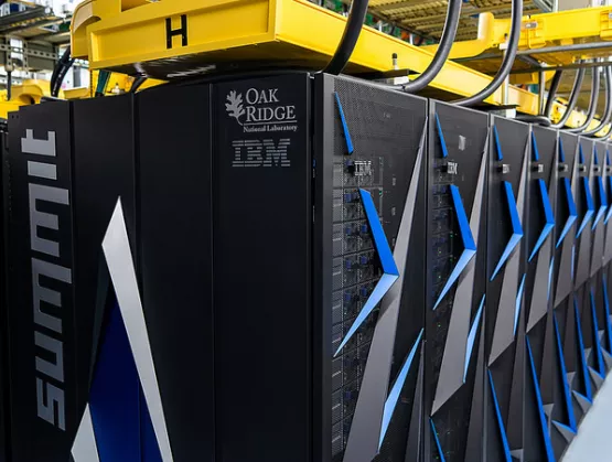
Post-Conference Report: SEMI Heterogeneous Integration SummitDemand for high-performance computing (HPC) chips is exploding. These super-speedy chips are critical for data centers and cloud computing infrastructures to support new performance-hungry technologies such as artificial intelligence (AI) and 5G. The challenge is for the devices and their multi-core architectures to couple high bandwidth density with low latency and high energy efficiency. Heterogenous integration offers a potential answer as an advanced packaging technology designed to meet these skyrocketing performance demands on HPC chips and open the door to a whole new world of 3D integrated circuits (ICs).So important are 3D ICs that Intel and TSMC representatives speaking at the recent Heterogeneous Integration Summit hosted by SEMI Taiwan in Taipei declared that the packaging technology will all but dictate the future of the industry. All told, 12 speakers from government, academia and a broad range of leading international companies from sectors including advanced packaging, design, manufacturing, silicon photonics, equipment and materials shared forward-looking strategies, the latest technologies and potential heterogeneous integration market opportunities. Koushik Banerjee, vice president, TMG, Assembly, and Test Technology Integration, at Intel pointed out that using heterogeneous integration for a single SiP (system-in-package) will deliver what the industry has long wanted by enabling multiple process nodes, more diverse silicon IP (intellectual property) and chip functionality, and chips that pair low energy with high frequency. Intel plans to announce its first Forveros 3D packaging product combining a 10nm HPC chiplet with a low-energy 22nm base die and stacked with memory on top. When asked about the future of advanced packaging technology, Banerjee said it will be very much about the combination of Foveros and its very own Embedded Multi-Die Interconnect Bridge (EMIB).For its part, TSMC, will continue to upgrade its CoWoS (Chip-on-Wafer-on-Substrate), InFO (Integrated Fan-out) and other 2.5D IC production solutions while developing 3D chip stacking technology such as SoIC and WoW (wafer-on-wafer). TSMC is ushering in a new age of 3D IC packaging, said Marvin Liao, Vice President, Backend Technology and Service Division, at TSMC. The company’s SoIC is based on Chip-on-Wafer concept, with the flexibility to support one-to-many or different process nodes, whereas its WoW integrates two wafers with solid yields that could be used for products of the same size or manufactured with mature process technology.Speakers also included representatives from ATOTECH, Lam Research, SPIL, Sigurd, Cadence, Grand Process Technology, ITRI (Industrial Technology Research Institute), Industrial Development Bureau, and Lee San-Liang, Distinguished Professor, Department of Electronic and Computer Engineering at National Taiwan University of Science and Technology all shared their perspectives on equipment, materials, and testing and how different industry value chains might contribute to the development of heterogeneous integration technology.Expected to be a key driver of the next wave of semiconductors, heterogeneous integration and related technologies – including 3D IC, FOWLP (Fan-out wafer-level packaging) / FOPLP (Fan-out panel-level packaging), silicon photonics, Micro LED, compound semiconductor, automated optical inspection and SLT (system level testing) – will be a key focus at SEMICON Taiwan 2019, September 18 to 20 in Taipei. The Heterogeneous Integration Innovation Zone – along with featured international programs such as SiP Global Summit, Strategic Materials Conference, the Smart Data Summit and the Smart Automotive Summit – will gather key industry players to reveal the latest technology breakthroughs and market trends.Emmy Yi is a senior marketing specialist at SEMI Taiwan.
Read More
The CPUs in Summit, the world's new fastest supercomputer are built on 14nm FinFET-on-SOI technology. Yes, those IBM Power9 CPUs are fabbed by GlobalFoundries (you'll also find them in the z14, the most recent in IBM's z-series of servers – a series that's been on various iterations of SOI since its launch in 2003, btw). Summit's at the U.S. Department of Energy’s Oak Ridge National Laboratory (ORNL) in Tennessee, USA. It is now the top US supercomputer, and it's for science. The IBM-built Summit currently claims the spot in the Top500 as the world's smartest and most powerful supercomputer. “It is capable of performing 200 quadrillion calculations per second — or 200 petaflops — making it the fastest in the world,” says IBM's Dr. John E. Kelly, III, SVP, Cognitive Solutions and IBM Research. “But this system has never been just about speed. Summit is also optimized for AI in a data-intense world. We designed a whole new heterogeneous architecture that integrates the robust data analysis of powerful IBM Power CPUs with the deep learning capabilities of GPUs. The result is unparalleled performance on critical new applications.” And if that's not impressive enough for you, it's also #5 on the Green500 list for the world's most energy-efficient computers, posting Power Efficiency (GFlops/watts) of 13.889. [caption id="attachment_11940" align="alignright" width="300"] Summit supercomputer nodes: The IBM-built Summit supercomputer is the world's smartest and most powerful AI machine. It consists of 4,600 individual nodes. Each node contains two 22-core 3.07GHz IBM POWER9 CPUs, which are built on GlobalFoundries' 14nm HP FinFET-on-SOI technology, as well as six NVIDIA Telsa GPUs. (Photo Credit: ORNL).[/caption] As GF noted when they announced the technology in the fall of 2017 (read the GF press release here), their 14HP is the industry’s only technology to integrate a FinFET transistor architecture on SOI. Featuring a 17-layer metal stack and more than eight billion transistors per chip, the technology leverages embedded DRAM and other innovative features to deliver higher performance, reduced energy, and better area scaling over previous generations to address a wide range of deep computing workloads. These technologies have long, deep histories (and were developed in close collaboration with SOI wafer leader Soitec). Here at ASN we have a fabulous archive of pieces contributed by IBM explaining the genesis of the technology – they're great reads and still entirely pertinent: FinFET on SOI: Potential Becomes Reality (by T.B. (Terry) Hook et al, 2013) – this presents the key technical data. IBM: Why Fin-on-Oxide (FOx/SOI) Is Well-Positioned to Deliver Optimal FinFET Value (by Terry Hook, 2012) – this great piece busts myths and clearly explains why FinFETs on SOI deliver top performance. IBM: FinFET Isolation Considerations and Ramifications – Bulk vs. SOI (by Terry Hook, 2013) – explains why and how SOI increases operating voltage range, simplifies processing, reduces variation, lowers soft error rate, and enables higher circuit density. Embedded Memories in SOI – (by Subramanian S. Iyer, 2006) explains the importance of SOI in the memory part of the chip design equation. [caption id="attachment_11939" align="alignleft" width="300"] The IBM POWER9 processor delivers unprecedented speeds for deep learning and AI workloads. IBM Engineer, Stefanie Chiras tests the IBM Power System server in Austin, Texas. (Photo Credit: Jack Plunkett/Feature Photo Service for IBM).[/caption] As ORNL noted in its press release (you can read it here), the first projects will apply machine learning and AI to astrophysics, materials science, cancer research and systems biology. BTW, Summit also has a slightly smaller sister machine called Sierra, going in at the Lawrence Livermore National Laboratory (part of the Department of Energy's National Nuclear Security Administration). With 4,320 nodes (each also containing two 22-core 3.07GHz IBM POWER9 CPUs, which are built on GlobalFoundries' 14nm HP FinFET-on-SOI technology, but just four NVIDIA Telsa GPUs), Sierra's claimed the #3 spot on the June 2018 Top500 list of the world's most powerful supercomputers. And the Power 9 is now finding it's way into major data centers – like Google's (read about that here). There have been some good pieces in the press about it, including in Forbes and The Motley Fool. So yes, clearly there are exciting markets for FinFETs on SOI!
Read More