downloadGroupGroupnoun_press release_995423_000000 copyGroupnoun_Feed_96767_000000Group 19noun_pictures_1817522_000000Member company iconResource item iconStore item iconGroup 19Group 19noun_Photo_2085192_000000 Copynoun_presentation_2096081_000000Group 19Group Copy 7noun_webinar_692730_000000Path
Skip to main content
Default Banner Image

machine vision

Japan’s semiconductor industry has weathered the COVID-19 pandemic to post robust growth. Far from a temporary setback, COVID-19 will lead to enduring change in how we work and live. And just as automation has been a bulwark against the devastating business impacts of the virus outbreak, increasing digitization will lead to new efficiencies in our industry.These were some of the key takeaways from three SEMI Japan Members Day webinars in June and July that offered the latest updates on COVID-19 impacts to the semiconductor industry and restart strategies for SEMI members. More than 2,000 SEMI members across Japan’s islands attended the webinars featuring the following five speakers: Hideki Kanewaka, Marketing Director, Consulting Lead, Japan, Accenture Japan Ltd. Takayuki Komori, Manager, Marketing Engineering Dept, SUMCO Corporation Taketoshi Hamaguchi, Director, Manufacturing Industry, Microsoft Corporation Akira Minamikawa, Senior Consulting Director, OMDIA (Informa Intelligence LCC) Yuichi Koshiba, Managing Director Partner, Boston Consulting Group COVID-19 Impact on Japan Semiconductor Industry is ModestThe consensus view of the five speakers from various quarters of the industry – consultant, IT service provider, materials supplier, market analyst – was that the Japan semiconductor industry withstood the heavy blows COVID-19 dealt to other industries thanks to strong demand for chips. Shelter-in-place policies and lockdowns spawned by COVID-19 has accelerated the digital transformation rippling around the world as electronics sales have soared to support everything from remote work and education to healthcare and home entertainment including gaming.The rapid growth of cloud usage for video streaming, gaming and remote work is taxing communications network capacity and placing more bandwidth demands on servers, said Akira Minamikawa of OMDIA. According to a recent report by Nokia, communications network traffic has skyrocketed 300 percent for online meetings and 400 percent for gaming, bringing the networks closer to their capacity limits. Minamikawa sees server shipments increasing at 8 percent CAGR through 2024. For the broader chip market, he expects demand for notebooks, solid state and hard disk drives, and gaming to remain strong in 2020. He also predicts rapid 5G penetration for smartphones will boost semiconductor chip industry growth.Still, not all semiconductor segments are expanding, said Yuichi Koshiba of Boston Consulting Group. Chip shipments for end products in markets such as automotive, industrial equipment and aircrafts are on the decline. Slowing demand for chips that power automotive applications in particular could pare sales for some chip companies and distributors since the segment accounts for a high proportion of their overall revenue.State of the Semiconductor IndustryFrom SUMCO’s vantagepoint as a major silicon wafer supplier, the company’s Takayuki Komori sees a number of changes unfolding in the semiconductor industry: Smartphones are driving growing demand for process technology (smaller nodes) and 300mm wafers. Komori estimates the typical high-end smartphone sports 1,700 square millimeters of silicon. 300mm wafers account for 80 percent of that total while more than 50 percent of the devices use leading edge multi-patterning technologies. Smartphones will need more RF chips to support 5G’s high-speed communications and added frequency ranges. Substrates for RF switches and tuners have been shifting from gallium arsenide (GaAs) and other compound semiconductors to silicon. 5G smartphone penetration will accelerate as the cost of integrating CPUs and modem functions into a single chip sees a swift decline. While the sensitivity and resolution of CMOS image sensors have evolved to incorporate innovative backside illumination and stacking technologies, future advances will focus more on products for machine vision applications capable of sensing invisible light bands. Rising adoption of electric vehicles and robotics applications will drive growing demand for power semiconductors that control their motors such as IGBTs and MOSFETs as the production capacity for the devices expands and shifts to 300mm wafer lines. For memory fabs, Minamikawa said utilization remains high as a result of a spending slowdown by major chip manufacturers and will stay elevated even once additional capacity ramps to support robust demand. Foundry fab utilization also remains high despite the pandemic-driven cancellation of smartphone chip orders in March. Minamikawa also sees the utilization rate of micro rising with the surge in demand for notebooks, PCs and servers in the second half of 2020.Transition to New NormalAs people around the world start to settle into new ways of living and working, there’s a growing acceptance that the transformation will be long-lasting. And no area of people’s lives is changing more than their work. Boosted by government subsidies, many small and midsize companies in Japan have started to implement work-from-home policies, an area where major electronics and IT businesses had already instituted reforms, said Hideki Kanewaka of Accenture. A few examples: Nippon Telegraph and Telephone Corporation (NTT) announced that half of its employees will continue to work from home in the future. A five-year plan Toshiba launched in 2019 to allow all employees to work from home will likely accelerate. Hitachi plans to allow all employees to work from home starting in April 2021. dwango, a major internet-based entertainment company in Japan, announced it will allow in principle any employees to work remotely. In the critical area of remote sales, Kanewaka pointed to the importance of going beyond online business meetings, paperless transactions and virtual events to devise new ways to attract customers and close deals. Creating online communities and providing rich digital content are also important measures to consider, he said.Manufacturing's Digital TransformationTravel restrictions by most countries to curb the COVID-19 outbreak have also raised barriers to chip companies sending engineers overseas sites to service state-of-art equipment and provide other technical support. Microsoft’s remote assist system deployed by ASML is one tool semiconductor makers can use to overcome this challenge, said Taketoshi Hamaguchi of Microsoft.The system connects a remote equipment service expert with an onsite worker through the internet, allowing the technical expert to provide support through a goggle display with a camera worn by the worker. Guided by the expert, the worker can perform complex services. A Natural User Interface (NUI) helps give the factory worker a clear understanding of the often highly technical instructions.Using artificial intelligence (AI) to increase automation will also help reduce the reliance of semiconductor factories on onsite workers. For example, AI deep learning can be deployed to calibrate equipment autonomously and reduce downtime after scheduled maintenances, Hamaguchi said.Corporate Restart Strategies Beyond factory considerations tied to COVID-19, semiconductor companies will need to adapt their business strategies to new ways of operating. For example, global supply chains will shift to domestic sources and increase redundancy to ensure a steady supply, a change leading to higher overall costs, Koshiba said. Trade routes among regions will also be redrawn as the trade rift between the United States and China and other geopolitical tensions intensify. The total value of those routes is expected to recover by 2023.Koshiba advised companies to evaluate the supply chain trade-offs between stability and cost and factor in potential risks to improve their short-term resilience and drive mid- to long-term supply chain restructuring.After past recessions, 14 percent of companies restored sales growth, Koshiba said. He recommended investing aggressively in growth and seizing M A opportunities during the downturn. Chip companies must also adapt to supply chain changes faster than competitors.Become a SEMI MemberWebinars like the recent SEMI Japan Members Day series have become increasingly important in the mix of programs and services SEMI offers members to help them connect, collaborate and innovate in the microelectronics community. To become a SEMI member, please visit the SEMI website or contact your nearest SEMI office.Jim Hamajima is president of SEMI Japan.
Read More
Sapphire is a precious gemstone, consisting of aluminum oxide (α-Al2O3) with occasional traces of other elements such as iron, titanium, chromium, vanadium or magnesium. While sapphire stones found in nature mostly go to jewelry applications, the lab-grown sapphire – produced in a scale of up to several hundred tons per year – is widely used by the electronic industry. Now one can hardly find a branch of technology where this crystal is not used.Sapphires are mainly applied in infrared optical components, high-durability windows, wristwatch crystals, and the very thin electronic wafers used as the insulating substrates of solid-state electronics. High thermal conductivity, low reactivity, and appropriate unit cell size make sapphire an ideal material for a wide range of such electronic substrates for manufacturing of components such as LEDs and CMOS chips.SEMI spoke with Ivan Orlov, CEO of Scientific Visual, after his presentation at SEMI Strategic Materials Conference at SEMICON Europa, 12-15 November, 2019 in Munich, Germany, to learn more about the future of sapphire.SEMI: Why is sapphire an ideal material for a wide range of electronic substrates? Orlov: Sapphire undoubted advantages are its chemical inertness and ability to withstand high temperature, radiation and mechanical loads. In addition, it exhibits low dielectric loss and very good electrical insulation that makes sapphire a good candidate for substrates for LEDs and laser diodes or wafers for epitaxial growth. However, the most important advantage is that sapphire crystal lattice does very well matching semiconductor materials deposited to its surface, in particular nitrides of group III elements. To plainly benefit from these features, the grown sapphire must have as few macro- and micro-defects as possible, as substrate defects are inherited by semiconductors layers grown on the substrate surface. Hence the importance to detect defects in the raw sapphire material. This is the area where our team at Scientific Visual contributes. SEMI: Flaws are usually identified only after costly wafering and polishing steps, because rough surface of raw crystals prevents detection of the defects. What can be done to prevent defects?Orlov: Today, major players are investing in growing larger crystals without mastering in depth the growth process. Let’s face it, the semiconductor substrate industry, which is primarily based in Asia, is using empirical research methods. The raw sapphire boules are still inspected manually, and this qualitative assessment is exploited in two folds. The first step is to further process the boule. Furnace operators then adjust the growing parameters depending on the results of the manual inspection.Due to the lack of visibility into internal crystal defects, the crystal growth and its downstream processing remain an art rather than a science. The primary reasons are the difficulty to measure, locate and quantify precisely the defects in the full crystal volume. Scientific Visual equipment enables defects in raw boules to be fully quantified and categorized. With such objective measurements and knowing the full set of growth parameters, the Process Engineering (PE) team can, with the assistance of deep learning algorithms, considerably improve the growing process. Our quality control tools give Process Engineering team the “eyes” to see complete defect distribution in raw crystals, enabling it to make minor modifications in the growth process to improve yields, reduce costs and shorten the time to market for products.SEMI: What lead to those advancements and what problems did your team set out to solve? Orlov: Breakthroughs in immersion tomography, machine vision and parallel computing drove advancements in automated quality control technology. Previously crystal inspection accuracy was limited by the acuity of the operator’s eye and subjective bias. Light distortion and the diffusion of crystals made it impossible to accurately identify internal defects.Scientific Visual equipment give operators an undistorted 3D view of all defects in a crystal boule or ingot. However, only deep learning technology can correlate a hundred thousand growth data points to identify a final defect pattern.Defect pattern in non-processed item cored from EFG sapphire plate. Well visible is a typical wavy pattern of surface layers and sandwich structure in the volume. Color code marks sapphire defect density: from deep blue (non-defective material) to deep red (highest defectiveness.) SEMI: What challenges are addressed by your approach? Orlov: Increasing the yield of semiconductor substrates like Sapphire, Gallium Nitride and Silicon Carbide is paramount to reducing the price of wafers while increasing their quality. The upstream growth and downstream wafering processes are not deterministic. So far, most of the producers can only determine the quality during the late stages of the process. This condition creates huge constraints for teams in charge of production and processing. Automated Quality Control (QC) at the early stage of the production chain relieves all the unknowns, ultimately reduce the cost of material.SEMI: And what are the main opportunities?Orlov: There are massive opportunities to increase the yield and to ease the full processing chain from growth to the wafering process. Objective Quality Control (OQC) paves the way to industry-wide standards that categorize crystal quality at each step of growth to enable full certification of the defectiveness of the material and facilitate its trade and exchange.SEMI: What’s one of your predictions for the future of new materials?Orlov: The explosion of e-mobility and electric vehicles and the development of other green technologies will drive rising demand for low-defect sapphire, silicon carbide and gallium nitride substrates thanks to the streamlining of the full processing chain. Manual quality control will soon give way to full automation as quality control in sapphire and other raw crystals production is the only missing link in a fully automated semiconductor production chain. I believe that in five years, automated raw crystal inspection will become standard in the industry. Our mission is to empower every crystal grower to achieve this important milestone.Dr. Ivan Orlov obtained a Ph.D. in Crystallography from the Federal University of Technology in Switzerland EPFL and an MSc in Solid-State Physics in Moscow, Russia. Ivan co-founded Scientific Visual in 2010 to answer the challenge of the synthetic crystals industry struggling with high defect yield. Prior to this he worked in a company specialized in diamond optics. He has more than 10 years of experience in R D with focus on optical materials, industrial crystals and non-destructive quality control technologies. Dr. Orlov was a SEMI Task Force member for sapphire standard development in China and collaborates with ISO committee in Switzerland to establish industry-wide sapphire quality standards.Serena Brischetto is senior marketing and communications manager at SEMI Europe.
Read More
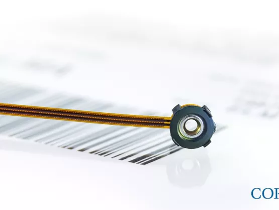
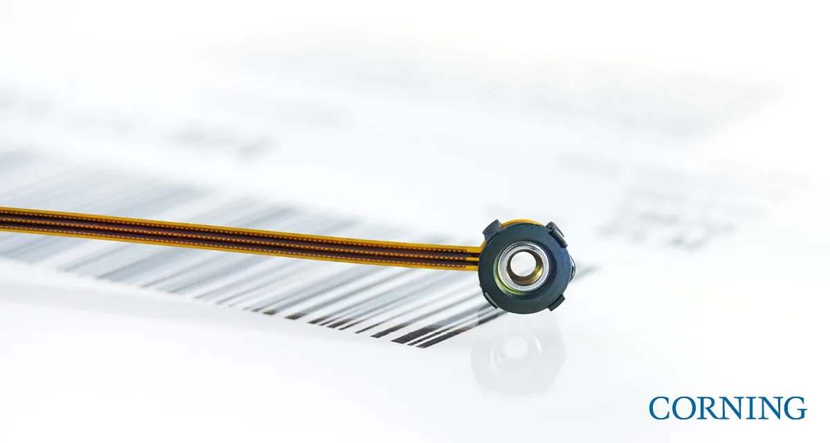
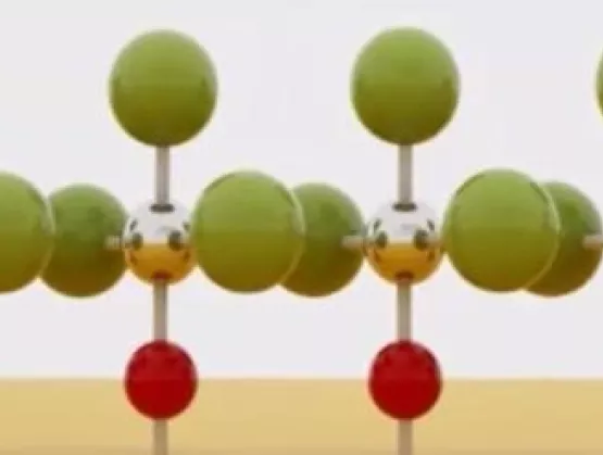
The evolution of industrial and non-industrial automation, smart manufacturing, and Industry 4.0 technologies have increased demand for vision systems that support robust, reliable imaging industrial applications. What factors are driving growth in the machine vision market today?SEMI spoke with Frederic Laune, Business Manager, European Technology, Corning, about how Corning® Varioptic® Lenses are vital to advancing the speed, efficiency, and integration of products using computer imaging. Laune shared his views ahead of his presentation at SEMI MEMS Imaging Sensors Summit, 25-27 September, 2019, at the WTC in Grenoble, France. Join us at the event to meet Corning and many other key industry influencing players. Registration is open.SEMI: Corning's markets include optical communications, mobile consumer electronics, display technology, automotive, and life sciences vessels. Back in June 2019, Corning Incorporated announced that it had delivered its 2 millionth Corning® Varioptic® Lens for industrial applications. What drove this great milestone?Laune: This milestone was met thanks to the fact that Corning Varioptic’s solution solves several problems generated by classical motorized solutions used in industrial applications: limited number of actuation cycles, poor vibration and shock resistance, size (meaning bulky), and high-power consumption. Before Varioptic, there was no variable focus solution that worked well.In addition, the explosion of the CMOS sensor technology helped drive down the cost of imaging solutions for industrial devices, increasing the number of applications and shipping volumes.SEMI: What inspired Corning Varioptic Lenses?Laune: Varioptic was started in 2002 by Dr. Bruno Berge, a French physicist turned entrepreneur. Inspired by the work of Gabriel Lippmann, the 1908 Nobel Prize winner for the invention of color photography, Dr. Berge explored the shape-altering effects of an electric charge when applied to two liquids, a phenomenon referred to as electrowetting. His research ultimately led to the creation of liquid lenses.Fast forward to 2017, when Varioptic became a part of Corning through an acquisition that included Varioptic and Invenios technologies. We believe the synergies from this acquisition will lead to exciting new liquid lens application opportunities that align with Corning’s growth strategy and core capabilities. Corning is one of the world’s leading innovators in materials science. For more than 165 years, Corning has applied its unparalleled expertise in glass science, ceramic science, and optical physics to develop products that transform industries and enhance people’s lives.SEMI: What differentiates traditional camera systems from adjustable lens solutions?Laune: Traditional industrial cameras are usually fixed focus, meaning that the image is sharp only in a limited distance range. Unlike consumer camera applications, there were no good solutions for variable or auto focus cameras in the industrial space. This is due to the intrinsic limitations of motorized technologies.Therefore, customers were using, for example, several cameras to focus at several distances. This compromises the optical quality by closing the objective in order to increase the depth of field, therefore limiting resolution and leading to a need for more light.The cameras using Corning Varioptic’s technology offer more functionality with their ability to focus, whatever the distance, in a fast, reliable, and accurate fashion, and with lower power consumption than traditional mechanical solutions. The upshot is that the product that can withstand heat, vibration, mechanical shocks, and high numbers of focus cycles in tough industrial environments. SEMI: And how is electrowetting enabling industrial devices to capture images and process information quickly and clearly? Laune: In two words: fast and accurate.Electrowetting has unique features – with our two-liquid solution, we combine fast focus with high vibration and shock resistance, and the added benefit of low power consumption.What’s more, our programmable lens can be reconfigured on demand. The lens adapts rapidly and continuously from diverging to converging and can be modeled to support demanding variable focus applications. Our lenses can change their focus in milliseconds, similar to the human eye, and capture fast-moving objects at varying distances. The use of liquid, over mechanical solutions, allows us to create a small form factor, saving precious space and reducing power consumption.SEMI: What industrial applications are taking advantage of this technology? Can you name one example?Laune: 2D barcode readers and industrial vision are our main markets. There is also a strong adoption of our technology in medical applications.SEMI: What does the rise of machine vision mean for manufacturers? Give us one prediction about the opportunities offered by advanced imaging applications.Laune: A great example is the use of 2D barcode readers and liquid lenses to track your ecommerce order, point to point. Another example is full product traceability by implementing a 2D barcode on every component of a given product globally to improve product quality. The varying and adjustable focus abilities of our liquid lens technology make it possible for barcode scanners to track products of different heights, allowing manufactures to improve their processes and logistics.Beyond these examples, tracking and analyzing are booming, thanks to the combination of low-cost CMOS sensor technology, increasing processing power, innovative algorithms (deep learning, AI, neuromorphic processors, etc.), and better image quality due to the progress of lens technology, Varioptic being one.We see an opportunity to improve people’s lives, such as enabling better analysis of medical images and improving the use of cameras in biomedical technologies.SEMI: Quality inspection and automation, adoption of Industrial 4.0 technologies, government initiatives. If you were to choose one, what main factor will drive growth in the machine vision market?Laune: It is difficult to pick just one. I believe that full traceability (monitoring individual parts throughout the production process) has interesting implications as compliance and regulatory efforts ramp up and stronger security of goods becomes more important, particularly as consumers become engaged in food safety and tracing products throughout the supply chain.SEMI: What are your expectations for the SEMI MEMS Imaging Sensors Summit and why would you invite your peers to attend? Laune: I strongly believe in the power of human interactions in technology and science! Ideas come from discussions and physical interactions. The SEMI MEMS Imaging Sensors Summit is a great place to network, meet people, and think about the future! Frederic Laune is the business manager leading the Corning® Varioptic® Lenses business. Laune joined Varioptic as an R D engineer in 2003 after spending the first eight years of his career developing novel active components for the optical telecom industry. At the time, Varioptic was a newly created start-up aiming to develop liquid lens technology for industrial applications. After designing the first two Varioptic commercial products, the Arctic 320 and Artic 416, Laune stepped up as head of Varioptic’s R D department to focus on product and performance improvements. In 2010, he was appointed sales and marketing lead for the company. Varioptic was acquired by Corning Incorporated in early 2017. Laune received a master’s degree in physics and optics from University Pierre and Marie Curie (Paris) in 1995.Serena Brischetto is a marketing and communications manager at SEMI Europe.
Read More
SEMI spoke with Dr. Mikko Söderlund, sales director for Beneq’s semiconductor business, about trends in Atomic Layer Deposition (ALD) applications. Söderlund shared his views ahead of his presentation at SEMI MEMS Imaging Sensors Summit, 25-27 September, 2019, at the WTC in Grenoble, France. Join us at the event to meet Beneq and other key industry influencers. Registration is open.SEMI: The Backside Illuminated (BSI) CMOS Image Sensors (CIS) market continues to experience steady growth. Which applications are currently driving market growth?Söderlund: BSI CMOS Image Sensor market continues to be driven by mobile, security, automotive and Internet of Things (IoT) applications – so there seems to be plenty of opportunities for BSI CIS market to grow further.SEMI: What is critical for advanced thin-film deposition methods to extract best electrical performance?Söderlund: It is critical to control the material properties of the deposited layer (such as charge density, resistivity or barrier property) and of course, film uniformity and conformality. Furthermore, controlling material interfaces is also important, especially for sensitive III-V materials. {% video_player "embed_player" overrideable=False, type='scriptV4', hide_playlist=True, viral_sharing=False, embed_button=False, width='350', height='197', player_id='12721134435', style='margin: 0px auto; display: block; float: right; margin-left: auto; margin-right: auto; width: 350px;' %} Coatings and material features based on existing standard techniques can be very expensive, or not feasible at all. What does Atomic Layer Deposition (ALD), as a thin film coating method, offer in particular?Söderlund: ALD offers dense, highly conformal and pinhole-free best-in-class functional layers for dielectrics, passivation, encapsulation and much more. As a gentle and precise layer-by-layer method, ALD is extremely well-suited for deposition of such performance critical layers over large surface areas such as a cassette of wafers.SEMI: Please describe the Atomic Layer Deposition (ALD) coating process. Söderlund: ALD is based on a self-limiting surface reaction controlled thin film deposition. During coating, two or more chemical vapors or gaseous precursors react sequentially on the substrate surface, producing a solid thin film (see schematic below). Most ALD coating systems use a flow-through traveling wave setup, where an inert carrier gas flows through the system and precursors are injected as very short pulses into this carrier flow. The carrier gas flow takes the precursor pulses as sequential waves through the reaction chamber, followed by a pumping line, filtering systems and, eventually, a vacuum pump.SEMI: What are the two leading edge ALD applications?Söderlund: Today’s leading-edge ALD applications are in logic (high-k/metal gate, multiple patterning) and memory (DRAM capacitor, 3D NAND). Within the More-than-Moore (MtM) markets, CIS and MEMS (actuators and sensors, RF) have been early adopters of ALD, and we also see ALD being introduced in GaN Power and RF, as well as photonics.SEMI: Give us one prediction about the opportunities offered by advanced imaging applications.Söderlund: The large diversity of imaging applications will continue to drive growth and innovation. For example, machine vision is expected to transform the imaging landscape. We see this as a big opportunity for advanced thin-film deposition methods such as ALD, provided that the tools are versatile enough to address the diverse manufacturing requirements.SEMI: What are your expectations for SEMI MEMS Imaging Sensors Summit and why do you invite your peers to attend? Söderlund: The summit brings together all key RF stakeholders in the MEMS and imaging sensors industry, and we are looking forward to a great event. It’s a special event for us as we are officially launching a new ALD cluster tool product specifically engineered for the MtM applications – so this brings great excitement that we want to share with the attendees.Dr. Mikko Söderlund is Sales Director for Beneq’s semiconductor business. He has more than 20 years of experience in product development, product management, technical sales and business development across the photonics, OLED, and semiconductor industries. Mikko received his Ph.D. in Micro- and Nanotechnology from the Helsinki University of Technology. Serena Brischetto is a marketing and communications manager at SEMI Europe.
Read More