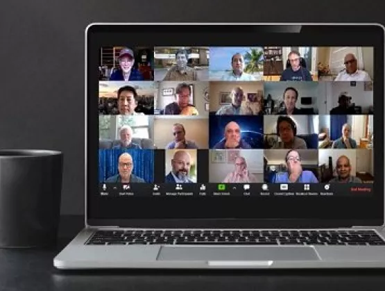
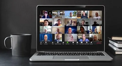
Tracking and quickly diagnosing COVID-19 infections, working from home and telemedicine recently came into sharp focus as technology executives and other subject matter experts from microelectronics heavyweights recently gathered for the first-ever virtual SEMI CTO Forum to explore how the microelectronics industry and their own companies can leverage future technology trends to drive growth.
Themed Intelligent Medtech and Wearable Technologies, the forum drew CTOs from ARM, Babblelabs, Brewer Science, Dell, Dow/Dupont, E-Ink, Hewlett Packard Enterprise, Intel, Lam Research, KLA, Microchip, ON Semiconductor, Qualcomm, Tokyo Electron, Ulvac, Veeco and Xilinx. The event is designed as a strategic driver of pre-competitive innovation. Following are key takeaways from the forum.
Microfluidics Promises to Speed COVID-19 Diagnosis
More than 240 companies worldwide are developing microfluidics solutions to improve diagnosis and treatment of COVID-19 and other conditions, said forum speaker Dr. Kurt Petersen, a member of Band of Angels, Silicon Valley's oldest angel investment group, with an illustrious background1 in technology.
And their innovations are bearing fruit. Cepheid, a company founded by Dr. Petersen, has developed a disposable microfluidic cartridge, Xpert Xpress SARS-CoV-2, used by doctors to swab the inside of a patient’s mouth. Highlighting the vital role of MEMS in medical electronics, the tiny powerful devices are behind a test that can detect COVID-19 infection in under 40 minutes. Dr. Petersen also cited a few examples of implantables and injectables under development, including:
In vivo chemical sensing: Profusa developed a continuous glucose monitoring sensor via an optical patch.
Glaucoma pressure monitors: Injectsense built a silicon chip the size of a grain of rice that is embedded in the eye to measure eye pressure.
Retinal implants: Second Sight implanted a 60-electrode array chip that projects images onto the retina to improve vision.
Microelectronics Takes Aim at Battling COVID-19
The event’s CTO roundtable, a platform for discussing societal and technology issues, revealed microelectronics technology will likely give rise to solutions for combatting pandemics and new business opportunities both in the short and long run. Areas of the greatest interest included:
Tracking and Security: Infection tracking accuracy is key to limiting the spread of viruses yet comes with inherent privacy and security challenges. The consensus view of the executives was that developing trusted hardware capabilities is critical for adoption of accurate infection-tracking technologies.
Remote Operation: Executives expect working from home or the use of telehealth to continue building momentum long after pandemic. To give staying power to the remote communications at the heart of these trends, microelectronics ecosystems will need to boost compute performance, both at the edge and in the cloud, while increasing bandwidth to enable applications such as augmented reality/virtual reality (AR/VR), artificial intelligence (AI), machine learning and advanced data analytics.
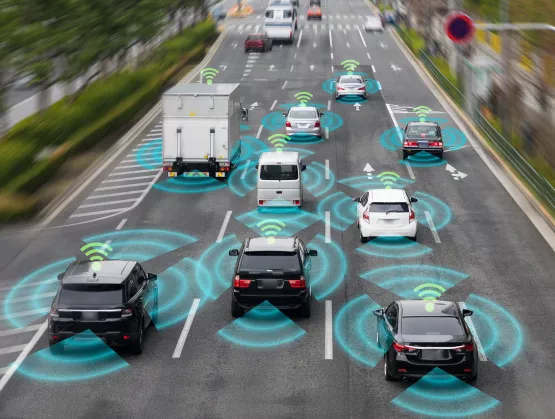
Edge intelligence: The challenge of remote communications spans both people and the Internet of Things (IoT). Questions persist about how hundreds of billions of sensors will connect to the cloud and how much power they will consume. The need to push computing to where data is generated – at the edge – is rising and the necessary underlying technologies will only come by combining various forms of distributed computing and analytics.
The microelectronics industry’s ability to seize these opportunities will only be possible with huge strides in innovation, raising concerns among the CTOs about the financial viability of cutting-edge devices because of increasing device complexity and R D costs. Technology partnerships and collaborations – an area where SEMI is contributing and will continue to expand its efforts as it works with the CTO community – will be critical to containing R D costs. SEMI will help the executives identify and mobilize the resources key to future innovation.
Improving Home, Work Productivity and Experiences Key to AR Adoption
Smart wearables also offer great promise. In just over a decade, AR and VR have grown from science fiction to practical uses such as AR applications for smart contact lenses, said Dr. Mike Wiemer, Co-Founder and CTO of Mojo Vision2.
Dr. Wiemer said that while many AR applications remain under development, the technology will only see widespread adoption once it starts to improve productivity and efficiency at home and work and the quality of other experiences. The smart augmented reality contact lens developed by Mojo Vision is a step in that direction. The product’s built-in display gives users timely information about everything they see while remaining invisible by packing 70,000 pixels into a space smaller than a half a millimeter across, making it the smallest and densest dynamic display ever made. The contact lens is powered by an ARM-based processor, with later versions adding an image sensor, eye-tracking sensors and a communications chip.
SEMI thanks EMD Performance Materials and Telit for sponsoring the CTO Forum. For more information on the CTO Forum and SEMI’s Smart Data-AI initiative, please sign up on our webpage.
1 Dr. Kurt Petersen is a member of the National Academy of Engineering, an IEEE Medal of Honor winner, and a Life Fellow of the IEEE for his contributions to the commercialization of MEMS technology.
2 Dr. Wiemer also co-founded Solar Junction, where he led technical teams to two world records in solar cell efficiency (43.5% and 44%). He also has patents and papers in Semiconductor Devices Applications, Silicon Photonics, Materials Integration, Lasers, Solar Cells, Solar Systems, and Analog Circuits.
Tom Salmon is Vice President of Collaborative Technology Platforms at SEMI. Pushkar P. Apte, Ph.D., is Strategic Technology Advisor for the Smart Data AI Initiative at SEMI.