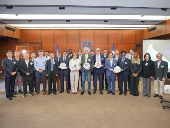
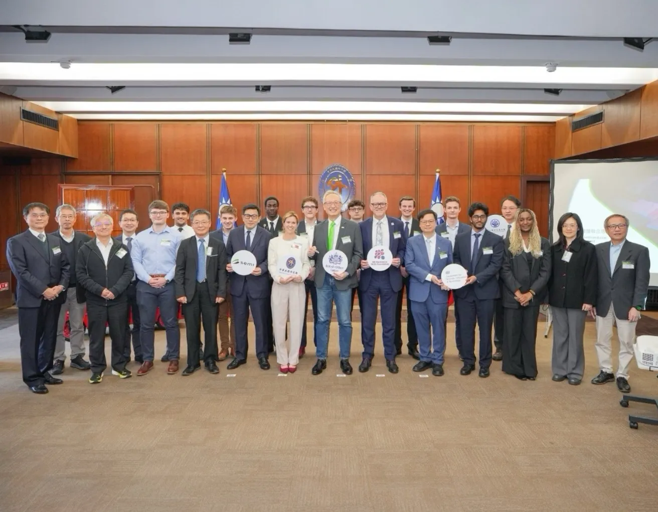
The global semiconductor industry is entering a new phase of growth to keep pace with the increasing demand for artificial intelligence (AI), high-performance computing (HPC), and system-level integration. At the same time, rapid technological advancement is intensifying the need for highly skilled talent. Industry projections indicate that by 2030, the global semiconductor sector will face a shortage of more than one million professionals, making talent a critical variable shaping competitiveness and supply chain resilience.In this context, governments and industry organizations worldwide are accelerating efforts to develop talent pipelines and strengthen cross-border collaboration. For a highly globalized industry like semiconductors, the movement of talent and exchange of knowledge are no longer confined to individual markets, but are essential to the development of a resilient and interconnected global ecosystem. Increasingly, competition is extending beyond technological breakthroughs to the ability to build and sustain a global talent pipeline.Supported by a cross-border collaboration framework, SEMI and the UK Electronics Skills Foundation (UKESF) have jointly organized a program to cultivate the next generation of semiconductor talent. Through structured exchange mechanisms and close collaboration with industry, academia and public sector partners, the program connects global talent with real-world industry environments and contributes to building a more sustainable foundation for long-term workforce development.From Lab to Fab: Understanding the Path from Research to ManufacturingA core objective of the project is to bridge the gap between academic research and industrial application. Through a 14-day immersive experience combining industry engagement and hybrid learning formats, participants engage directly with experts and gain a system-level understanding of how the semiconductor industry operates—from research and development to high-volume manufacturing.The program covers key segments of the semiconductor value chain, including advanced research, wafer fabrication, IC design, packaging and testing, and system applications. This integrated learning experience enables participants to move beyond isolated technical knowledge and develop a broader understanding of how innovation is translated into scalable industrial capabilities.As one participant shared: “Experiencing the award-winning R D solutions at ITRI and the massive scale of wafer manufacturing at UMC firsthand was unforgettable. It was incredibly inspiring to see how advanced research is translated into global manufacturing capabilities—from lab to fab.”Participant feedback highlights a clear shift in understanding. Through hands-on learning and industry engagement, participants moved beyond isolated technical knowledge to develop a more comprehensive, system-level perspective of the semiconductor industry—supporting more effective collaboration across the global ecosystem.A Practice-Oriented Approach: Redefining Semiconductor Talent DevelopmentAs technology evolves and industry demands shift, traditional discipline-based education models are no longer sufficient to fully meet the needs of semiconductor manufacturing and R D environments. Increasingly, the industry is seeking talent with cross-disciplinary capabilities and hands-on experience.The project adopts a “learning by doing” approach, combining laboratory sessions, expert-led workshops, and company visits to provide participants with practical exposure to semiconductor devices, materials, process technologies, and system design. Participants also gain exposure to real-world applications such as chip security, design verification, and advanced process technologies.From an industry perspective, this approach aligns more closely with evolving workforce needs. Compared with conventional academic training, individuals with cross-disciplinary experience and international exposure are better equipped to understand the interplay between R D and manufacturing, and to integrate more effectively into real-world operational environments.UK participants, dressed in cleanroom suits, gained firsthand exposure to Taiwan’s semiconductor manufacturing environment—observing wafer fabrication equipment up close and engaging in hands-on learning to experience the journey from lab to fab.From Talent Development to Ecosystem ConnectivityAt a time when the semiconductor industry is entering its next phase of growth, talent plays a central role not only in driving innovation, but also in enabling global collaboration. As supply chains become increasingly interconnected, building mechanisms for cross-border talent mobility and cooperation is critical to strengthening both resilience and innovation capacity.At the program’s closing event, “UK–Taiwan Semiconductor Industry and Talent Exchange,” Terry Tsao, Global Chief Marketing Officer and President of Taiwan, SEMI, noted:“By 2030, the semiconductor industry is expected to require more than one million additional skilled professionals. Through international collaboration and industry–academia engagement, SEMI aims to enable more global talent to engage with Taiwan, gain a deeper understanding of its semiconductor ecosystem, and build long-term connections with the industry.”The project reflects a broader objective: not only to develop talent, but to build a sustainable, globally connected workforce network. By fostering a shared understanding and collaboration across borders, such initiatives help align capabilities and drive innovation across the global semiconductor ecosystem.Terry Tsao, Global Chief Marketing Officer and President of Taiwan, SEMI, emphasized the importance of nurturing globally connected semiconductor talent to help drive the industry’s future growth.Advancing Global Collaboration to Meet Long-Term Industry NeedsAs the industry continues to evolve, no single organization or region can address workforce challenges alone. Cross-border collaboration and structured talent development frameworks will be essential infrastructure for the future of the semiconductor industry.Looking ahead, SEMI will continue to expand international partnerships, connecting global industry, academia, and government stakeholders to deepen and scale talent development efforts—supporting the next generation of semiconductor professionals with both global perspective and practical expertise.For more information or partnership opportunities, please contact:Ily TsaiTel: +886-3-560-1777 [email protected] Ily Tsai is Project Manager, Workforce Development at SEMI Taiwan.