downloadGroupGroupnoun_press release_995423_000000 copyGroupnoun_Feed_96767_000000Group 19noun_pictures_1817522_000000Member company iconResource item iconStore item iconGroup 19Group 19noun_Photo_2085192_000000 Copynoun_presentation_2096081_000000Group 19Group Copy 7noun_webinar_692730_000000Path
Skip to main content
Default Banner Image

Germany

SEMI spoke with Dr. Franz Laermer, Research Fellow (Senior Chief Expert) at Robert Bosch GmbH Stuttgart, Corporate Sector Research and Advance Engineering, about the latest trends in medical diagnostics and personalized treatments. An open platform for the automation of complex molecular diagnostics workflows recently developed by Robert Bosch has proven its ability to take molecular diagnostics to the point of need.To make this happen, miniaturization, microsystems and microfluidics technologies, as well as microelectronics, are crucial. This is critical for the detection of SARS-CoV-2 infections within a rather short development time.Laermer shared his views ahead of his presentation at the SEMI MedTech Forum, 19 February, as part of the SEMI Technology Unites Global Summit, 15-19 February 2021, online event. Join us to meet experts from Robert Bosch and other key industry influencers. Registration is open. SEMI: What is driving innovation in diagnostics and what role does the semiconductor industry play?Laermer: One of the major drivers in diagnostics is the molecular breakdown and detailed analysis of nucleic acids on the level of the individual nucleotide. This reveals the root causes of diseases like cancer, genetic aberrations, infections and therapy resistances. Today’s solutions are mostly PCR-based (that rely on the polymerase chain reaction) or depend on sequencing. The keys to bring these technologies closer to the point of need are automation, miniaturization, low-cost, ease of use, flexibility, reliability, and fast time from sample-to-result. Semiconductor and microsystems technologies are enablers to meet these requirements, thanks to their ever-increasing performance, with Moore’s law pushing the semiconductor side of the story.SEMI: Can you tell us more about the the Bosch VIVALYTIC system? Laermer: VIVALYTIC is a universal and highly flexible diagnostic platform for the integration and automation of a wide variety of molecular diagnostics assays. It consists of the universal laboratory analyzer tool, which operates the application-specific cartridges. All reagents and specific bio contents are contained in the application-specific cartridges in a long-term stable manner at room temperature. The user only has to introduce the patient sample into the cartridge, push the cartridge into the analyzer and start the automatic workflow, which yields a diagnostic result within typically less than one hour. The VIVALYTIC products are manufactured by Bosch Healthcare Solutions GmbH (BHCS) in cooperation with strategic diagnostic partners and bio content owners.SEMI: How is the pandemic impacting automated diagnostics in the medical industry? What is new now?Laermer: The pandemic has clearly shown the importance of fast automated diagnostics at the point of need. Breaking infection chains as early as possible requires fast reliable PCR testing anywhere and anytime. We managed to reduce the time needed for SARS-CoV-2 rapid testing to less than 30 minutes for positive probes, an achievement that is embraced by our customers. Until a sufficiently high level of immunization is reached by vaccination, rapid testing is the only way to limit the number of infections, hospitalizations, and lethal outcomes of the COVID-19 pandemic.SEMI: Besides infectious disease diagnostics, what solutions will enable a paradigm shift in medical treatments?Laermer: Today more and more targeted drugs and therapies are developed in oncology to address certain mutations that are considered drivers of the cancer. This moves away from the one drug fits all approach to precision oncology. As a prerequisite of this personalized therapy, the mutation status of a tumor must be clarified – and monitored precisely and repetitively during therapy. The latter requires molecular diagnostics at the point of need, i.e. at the onco-ambulance. One keyword in this context is liquid biopsy. Another example of personalized therapy is the detection of bacteria type and antibiotics resistances in bacterial infections, and the selection of optimized antibiotics therapy.SEMI: What solutions can Robert Bosch bring to address the needs just mentioned? Laermer: Robert Bosch GmbH is a leader in microsystems, microsensors and semiconductor technologies. Our new 12-inch semiconductor plant in Dresden will strengthen our position in these fields. This encompasses artificial intelligence and the Internet of Things as well. As a technology provider, we generate superior solutions for automation and management of complex workflows, and thus deliver win-win-solutions together with our diagnostic partners.SEMI: How can technology unite us? Laermer: Technology, especially semiconductor and microsystems technology, is a game changer in the medical area. Whenever different disciplines meet each other and cooperate, as are the medical, diagnostics and semiconductor areas, innovation is accelerated strongly. New things happen at the interfaces between different areas of competencies.Franz Laermer, Research Fellow (Senior Chief Expert), Robert Bosch GmbH Stuttgart, Corporate Sector Research Advance Engineering. Dr. Franz Laermer joined the Corporate Research and Technology Center of Robert Bosch GmbH, Stuttgart, Germany, in 1990, where he started the development of new key technologies and sensor functions for the upcoming field of MEMS at Bosch. Today he is a Bosch Research Fellow/Senior Chief Expert for Microsystems, Microfluidics and Molecular Diagnostics. Laermer's work laid the foundation for the VIVALYTIC Diagnostics Platform of the newly founded Bosch Healthcare Solutions (BHCS) Business Division and the SARS-CoV-2 rapid tests from Bosch. Dr. Franz Laermer is the co-inventor of the Bosch Deep Reactive Ion Etching Process (BOSCH-DRIE) for microstructuring silicon. He holds more than 200 patents and was awarded with European Inventor of the Year 2007 – Category Industry prize by the European Commission and the European Patent Office (together with co-inventor Andrea Urban) for the invention, development and sustainable success of the BOSCH-DRIE process. He received the 2014 IEEE Jun-ichi Nishizawa Medal Award from the Institute of Electrical and Electronics Engineers (IEEE), USA. In 2019 he was awarded with the 2019 Technology Prize from the Eduard-Rhein-Foundation in Germany.Serena Brischetto is senior manager of Marketing and Communications at SEMI Europe.
Read More
In an important step toward resuming business as usual in Japan, Prime Minister Shinzo Abe on May 14 lifted the state of emergency originally scheduled to expire at the end of May for 39 of Japan’s 47 prefectures, marking “the real beginning of our efforts toward a new normal in the era of the coronavirus” as new cases continue to decline. But with Tokyo, Osaka and six other prefectures still under the state of emergency, Abe urged citizens to remain cautious as the nation and world continue to confront the COVID-19 threat. Among criteria the remaining prefectures must meet for a state of emergency suspension is a reduction in new infections to no more than 0.5 cases weekly for every 100,000 citizens. The eight prefectures account for nearly half of Japan’s population and GDP, with Tokyo and Osaka the two largest urban areas in the island nation. Japan expects to contain its economic losses to 38 trillion yen, 15 percent less than the 45 trillion yen hit originally projected. The Japan government has planned a May 21 progress review[1] in the eight prefectures, a timeline that Abe said could lead to the lifting of the state of emergency before the original cutoff at the end of the month, a move that would help stem the drain on the domestic economy.Strict Immigration Controls Restricts International Travel to and from Japan by Supplier EngineersAs I reported on April 21, the Japan Foreign Ministry on March 31 raised its travel advisory to level 3 for 49 regions around the world including the U.S., prohibiting travel from Japan for any purpose. SEMI Japan is urging government officials to exempt Japanese supply chain engineers from the travel ban to allow visits to semiconductor manufacturing facilities in those regions in order to install, start up and service equipment.Starting May 14, Japan blocked immigration of foreign nationals and permanent residents from 100 countries and regions worldwide, a ban applying to anyone who spent time in their home region within 14 days of their planned arrival in Japan. The areas include China, Singapore, South Korea, and Taiwan in Asia; Canada and the U.S.; and Germany, France, Italy, Netherlands, Switzerland and the U.K. in Europe. For the complete list, see the Japan Ministry of Justice’s website.Japan’s immigration ban mirrors restrictions now in place in many other regions around the world. The immigration controls are well-intended – to restrict the spread of COVID-19 – but hamstring the global microelectronics supply chain. For example, the curbs bar engineers from international travel to install new tools and software in fabs. SEMI Japan has stressed the potential chip industry impacts of the ban in ongoing talks with the Ministry of Economy, Trade and Industry and is facilitating discussions between government representatives and SEMI members to help clear the way for travel by critical supply chain workers to Japan. SEMI Supports Members with COVID-19 ResourcesSEMI international headquarters and regional offices are here to help you, our members. For more information on our webinars, surveys, best practices and other information designed to help you meet the challenges of the pandemic, please visit the SEMI Coronavirus Updates Resources page.[1] The May 21 review found three prefectures in western area – Hyogo, Kyoto and Osaka – met the criteria to lift the state of the emergency. Four other prefectures – Chiba, Hokkaido, Saitama and Tokyo – remain under the emergency order that will be reviewed again as early as May 25.Jim Hamajima is president of SEMI Japan.
Read More
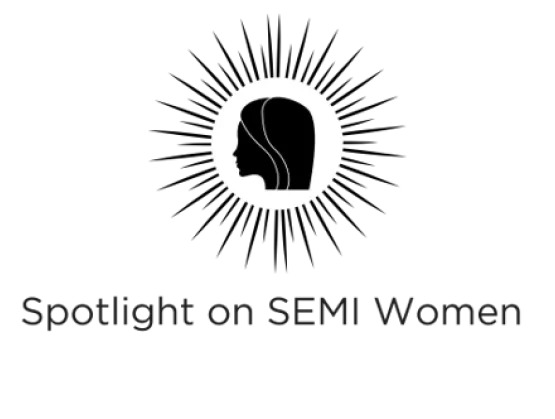
SEMI is excited to recognize Amy Leong, Chief Marketing Officer and Senior Vice President, Mergers and Acquisitions at FormFactor, as the SEMI Spotlight on Women Honoree for Q1 2020!Spotlight on SEMI Women celebrates the many accomplished women who work in the global microelectronics industry. Nominees in the quarterly spotlight include women who are beacons of knowledge, leaders of organizations and initiatives, hidden heroes and innovators in our industry. They are volunteers, protectors, intellectual disruptors and activists. Learn how you can nominate a woman for Spotlight on SEMI Women.An accomplished technology executive, Amy Leong has been an invaluable leader and role model at FormFactor for over a decade. During her tenure at Formfactor, Amy has led numerous successful new‐technology adoption and customer‐penetration initiatives that have helped drive FormFactor’s market share and profitability gains. Recently, she assumed oversight of the company’s M A strategy and execution.Amy is on the advisory board of the China International Semiconductor Executive Summit (CISES) and is a committee member for both the Semiconductor Wafer Test Workshop (SWTW) and the SEMI Industry Strategy Symposium (ISS) organizing group. Amy is an accomplished, engaging speaker and has presented at industry conferences and events. As a leader and role model, she shares her experiences and lessons as a successful technology executive, coaching peers and mentoring younger women to help overcome the challenges of building their careers in the semiconductor industry. Recently, Amy broadened these efforts by spearheading the formation of FormFactor’s b3.wn Women’s Network, a group of more than 120 FormFactor employees designed to gather and solidify the community of women at FormFactor.SEMI sat down with Amy to get some insights into her success.SEMI: Tell me about your background?Leong: I was born and raised in Tianjin, China and came to United States with my family when I was 16 years old. I always liked math and science growing up, which led me to pursue an undergraduate degree in chemical engineering at UC Berkeley and then enter the semiconductor industry. My work inspired me and, with the support of my employer, I earned my masters in Material Science and Engineering at Stanford University.SEMI: How did you get into the industry?Leong: At the time of my graduation, I had been considering several career paths and industries that were open to me because of my degree. Several of my peers had already joined the semiconductor industry and told me about the amazing technology they were helping to build. Once I entered the industry, the more I worked, the more fascinated I became with the fast pace of technology and innovation. Every year there were new opportunities to innovate that came with their own exciting challenges and problems to solve. I’ve now been in the industry for 22 years and I still love what I do.SEMI: Tell me about an accomplishment you are proud of?Leong: I have been at FormFactor twice now for cumulatively over 15 years. During my current tenure of about 10 years I have worked under Mike Slessor, our CEO. What I am most proud of is my commitment to professional growth by taking on new challenges. During my time at FormFactor I have jumped on opportunities to help solve challenges in different areas of the organization. Because I pushed myself into these new challenges and experiences, I have become a versatile leader with expertise in multiple areas within the business. I remember I started in product marketing, but when a sales account manager left a need in the business, I stepped in to help the customer and found my hidden talent of customer engagement and relationship building. When we urgently needed a new supplier for product development, I drove the supplier qualification and ramp up, and learned many aspects in operations. Of course without Mike allowing and encouraging me to stretch my skills in different directions, I would not be who I am today.SEMI: Is this strategy how you ended up in the M A space for FormFactor?Leong: My role now happened through a combination of organic and planned career opportunities. M A is a key component of the FormFactor growth strategy. When Mike needed help in the new space, I was able to volunteer, and relied on the knowledge and support of our board members and our executive team in order to meaningfully contribute to our M A strategies and executionMy mentality is to always get out of my own comfort zones. If you try and fail, so what? You learn, and you improve from your setbacks. But unless you try you will never know.SEMI: You have done so much for women in the industry and at FormFactor. What drives you to do this work?Leong: There are two primary driving moments in recent years that pushed me to step up.When Ajit Manocha joined SEMI, he started raising awareness of the importance of female leaders in tackling the industry’s challenges. While I had industry visibility, I wasn’t aware that the number of women in technology shrinks alarmingly the higher up the chain of command you look. My optimistic view is that we have a nearly balanced talent pipeline at the entry-levels, and there is great opportunity for the industry to take action and change the disheartening decline in female representation by mid-career.The second moment was a personal experience. In 2015, Formfactor hired our first woman board of director Kelley Steven-Waiss. (We now have three women board members.) Having Kelley on the board and leaning on her experience when I needed guidance showed me the power of having a mentor and a role model. Having somebody there as a sounding board was extremely helpful, and this triggered me to learn more about women leadership in technology and led me to want to do more for other women who were earlier in their career.SEMI’s influence was one of the major turning points in our industry and created a clarity that was not present by putting data in front of leaders for a powerful impact.SEMI: Tell be about the process of building the network of women at FormFactor?Leong: FormFactor’s women network grew mostly through a grassroots approach. A year ago, during a QBR (Quarterly Business Review) week, I had an opportunity to get together with a group of FormFactor female sales leaders. We had a wonderful evening together, shared our experiences and learned from each other. Our conversation left an impression on us, and we decided to start a women’s networking group at FormFactor so that more women can join the conversation. We named it b3.wn – Beautiful (be confident in ourselves and kind to others) Brilliant (make smart decisions) Bold (be fearless) Women Network. These three B words are the empowering characteristics of modern women to achieve our highest happiness potential at work, home and society. We had a modest goal for the group: Provide an informal venue for employees to engage, support and learn from each other. Little did we anticipate how quickly it would gather steam. Before long, we took the initiative on the road and hosted several events at our California and Oregon sites, featuring themes that ranged from women leadership panel discussion, to FormFactor executive chats on strategies to improve work and life balance and master effective business communications. One year later we now have over 120 members.This year we are going to expand the program into Asia and Germany as well! Global expansion is an exciting step and we are getting strong support from global sites. I think people are seeing the benefits of knowing there are colleagues or friends out there that share the same sets of work life challenges and you can seek support and help from each other.We need to be the change we want to see. I hope more of us can help support women in tech and create a more inclusive work environment at your company.SEMI: What advice would you give to people looking to grow their careers?Leong: Fearlessly step out of your comfort zone. When you are far outside your element, you can discover the new skills and strengths that you didn’t know existed before. It’s a super fun adventure, but you need to expect and embrace the failures that may come along the way, learn from them, and keep going. By continuously pushing the boundaries of our comfort zone, we can expand our horizon beyond what we once thought was possible.Cristina Sandoval is manager of Workforce Development at SEMI.
Read More
The combination of state-of-the-art semiconductor devices and upcoming manufacturing technologies for cost-effective processing of flexible film substrates has paved the way for a large variety of new applications in the emerging Flexible Hybrid Electronics (FHE).SEMI spoke with Professor Christoph Kutter, executive director, Fraunhofer EMFT, about current FHE technologies and market opportunities ahead of the Get Started with Flexible Hybrid Electronics workshop organized by Fraunhofer EMFT and supported by SEMI, 15 October, 2019, in Munich, Germany. To register for the event, click here.SEMI: Recent developments in thin semiconductors, new materials and cost-effective processing techniques have opened the door to a plurality of new applications and future products. What are the most innovative integration approaches?Kutter: Most interesting is the hybrid integration approach – the combination of most modern printing technologies and lithographically defined semi-additive copper wiring systems with state-of-the-art semiconductor components. Combining these best-of-breed technologies enables low-cost and high-volume printing but also ultra-low power electronics, which is important for every wireless device without or with limited power supply.SEMI: Integrating sensors, integrated circuits (IC), displays, antennas and communication devices on film substrates enables extremely thin and bendable form factors for applications where existing board-level technologies fall short. What are the key enabler technologies?Kutter: Key enabling technologies are fabrication of high-performance wiring patterns, integration of ultra-thin bare dies/components and ongoing advancements in roll-to-roll processing of film substrates. Besides the manufacturing technologies, materials such as electronic inks, substrates, isolation and passivation layers play a key role.SEMI: Are you currently working and experimenting on something particularly exciting?Kutter: We are in the process of developing an adaptive roll-to-roll direct imaging system that analyzes the position of the components manufactured before adaptive lithography steps are carried out in real time. We think that this concept will open up completely new processing possibilities for us. The technical infrastructure making this development possible is funded within the framework of the Research Fab Microelectronics Germany (FMD), the largest cross-site R D cooperation for microelectronics and nanoelectronics in Europe.SEMI: Can you share some details about the Fraunhofer EMFT roadmap?Kutter: Fraunhofer will push the hybrid integration – for example, combining printing technologies with high-performance CMOS – since we are convinced that hybrid integration is the only way to offer low-power systems for IoT with the highest performance and at the lowest cost. For this purpose, we are currently setting up a roll-to-roll die bond and component assembly machine.SEMI: What are your expectations for the future of flexible electronics and why would you recommend attending the workshop in Munich?Kutter: Flexible hybrid integration is becoming more important and offers the best of both worlds: mass volume printing technologies integrated with high performance ultra-low power electronics. You will see many examples of hybrid integration approaches during the workshop. This is a very important opportunity to highlight the latest developments in the semiconductor industry. Researchers, market analysts, material and product developers, and equipment suppliers will gather to provide insights into the latest flexible hybrid electronics innovations. We are particularly proud to organize this platform with SEMI and FlexTech Alliance.Agenda - Get Started with Flexible Hybrid ElectronicsLocation: Fraunhofer EMFT, Hansastrasse 27d, 80686 Munich, GermanyConference Chair: Prof. Dr. Christoph KutterENTRANCE Fees: 150 € VAT excl.Contact: [email protected] Prof. Dr. Christoph Kutter is the director of the Fraunhofer EMFT, focusing on sensing technologies based on silicon electronics and flexible hybrid integration technologies.Kutter completed his physics studies at TU Munich. In 1995, he earned his doctorate in physics at the University of Konstanz. Serena Brischetto is a marketing and communications manager at SEMI Europe.
Read More
Storage and memory chipmaker and SEMI China member Tsinghua Unigroup is gearing up to meet burgeoning product demand with huge investments in its manufacturing plants. But the high-tech enterprise under Tsinghua University is eyeing a much bigger prize – growth of the region’s semiconductor industry and the realization of its ambition to become a more prominent force on the global stage.Inspired by the national strategy, the Tsinghua Unigroup’s big spends include USD 24 billion in Wuhan (Yangtze Memory Technologies Co., Ltd.,) USD 30 billion in Chengdu, USD 30 billion in Nanjing and USD 100 billion in Chongqing, said Liu Hongyu, senior vice president of Tsinghua Unigroup, speaking at the SEMI China Equipment and Materials Committee meeting last month.Advanced packaging is another rich vein of opportunity the region is tapping for expansion, said Liu Hongjun, vice president of China Wafer Level CSP Co., Ltd., another SEMI China member attending the event, hosted by NAURA in Beijing. Hongjun sees strong growth for Fan-in, Fan-out, FCBGA, 2.5D and 3DIC, with Fan-out out front. Liang Sheng, administrative commission director at BDA, a business advisory firm supporting high-technology manufacturing in the E-Town economic development zone, pointed to 5G chips and smart, networked electric automobiles as drivers of the next growth phase of Beijing’s integrated circuit (IC) industry.Global tailwinds are lifting China’s semiconductor industry and the region’s hopes, with SEMI and major industry analysts raising their semiconductor industry growth projects for 2018 to between 9 percent and 16 percent. According to SEMI’s latest market report, global semiconductor industry manufacturing equipment revenue reached USD 17 billion in the first quarter of 2018, logging all-time highs after jumping 12 percent from the previous quarter and 30 percent year-over-year. Korea was the top-performing region at USD 6.26 billion, followed by China at USD 2.64 billion.Tighter integration with the rest of the global semiconductor industry is critical to the growth of China’s chip sector, and SEMI China is squarely focused on this assimilation, said SEMI China president Lung Chu. The spearhead of this effort is the SEMI Innovation Investment Platform (SIIP) China, established by SEMI China last year to help grow China’s pool of skilled workers, promote advanced technology, generate industry capital, and expand China’s semiconductor industry while developing stronger connections with chip sectors in other regions. To strengthen ties with other regions, SIIP China will stage a number of innovation and investment forums this year including Chinese Night at SEMICON West (July 10-12) and a SIIP China Forum in Silicon Valley (July 15). In August, representatives from the Korea chip industry will visit counterparts in China (August), and a China delegation will travel to Japan for meetings (October). SIIP China is also strengthening the region’s links with Germany and Israel as SEMI serves as a crucial bridge between China’s semiconductor sector and the global industry.At the invitation of Shanghai authorities and the Ministry of Commerce of the People’s Republic of China, SEMI China in November will join the China International Export Import Exposition in Shanghai, an event that will underscore China’s commitment to the openness and cooperation of its semiconductor industry with the international chip community. As part of the exposition, SEMI will work with the Ministry of Commerce and domestic chip manufacturers to begin development of a special integrated circuit (IC) zone. SEMI China members are welcome to participate.With workforce development no less vital to the future of China’s semiconductor industry, the Equipment Materials Committee offered potential solutions to the industry’s talent gap. Measures included targeting university students and engineers with industry lectures and courses in key cities, campus recruiting, talent training that members said they are willing to help SEMI coordinate and stage and, much like the push to better integrate China with the global semiconductor industry, mobilizing member resources around a campaign to polish the image of the industry to make it more attractive to students and young workers. Members of the SEMI China Equipment Material Committee gathered at NAURA in Beijing in June for a warm and lively discussion about global semiconductor industry cooperation and growing China’s semiconductor sector.Cherry Sun is a marketing manager at SEMI China.
Read More