
Setting the Standard: Advancing Test Methods for Particle and Contamination Analysis in Semiconductor Wafer Processing and Inspection
By Mayura Padmanabhan, SEMI
Particle contamination in the critical chamber components (CCC) of semiconductor wafer processing and inspection equipment can have severe repercussions on the yield and reliability of the resulting wafers and devices. To ensure the quality of their processing equipment, suppliers must establish measurement methods for particles that can be applied to various components within the line of sight of the wafers.
Controlling particles contamination on these components has become an essential quality requirement for users of the processing equipment. Therefore, standardizing the measurement methods and procedures is crucial to facilitate better communication between the supplier and the user.
The Semiconductor Component, Instrumentation & Subsystems (SCIS) Working Group's CCC and Particles Subcommittee has proposed two test methods for measuring surface contamination. These methods are currently being developed as SEMI Standards under the guidance of the Metrics North America Technical Committee Chapter.

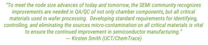
Test Method 1: Ultrasonic Aided Ultra-Pure Water Extraction Followed by Liquid Particles Counter for Particle Counts – developed by Kirsten Smith, UCT/ChemTrace
This test method describes the analytical methods for determining the extractable particles from CCC by ultrasonic- aided ultra-pure water (UPW) extraction followed by a liquid particle counter (LPC) for particle count and size measurements.
In a certified ISO 6 cleanroom environment, a CCC or coupon is immersed in an UPW filled precleaned and prequalified extraction vessel where ultrasonic energy is applied to extract both the surface and the partially embedded particles. The extraction solution is then analyzed by LPC. Applying consistent ultrasonic power, time, sample placement, and water volume across measurements and LPC make, and model is critical for comparing CCCs or coupons from the same substrate, surface treatment and coating. For each particle size, typically >0.2, >0.3, >0.5, >1.0 and >2.0mm (however this may vary), particle counts are calculated and reported in particles/cm2.
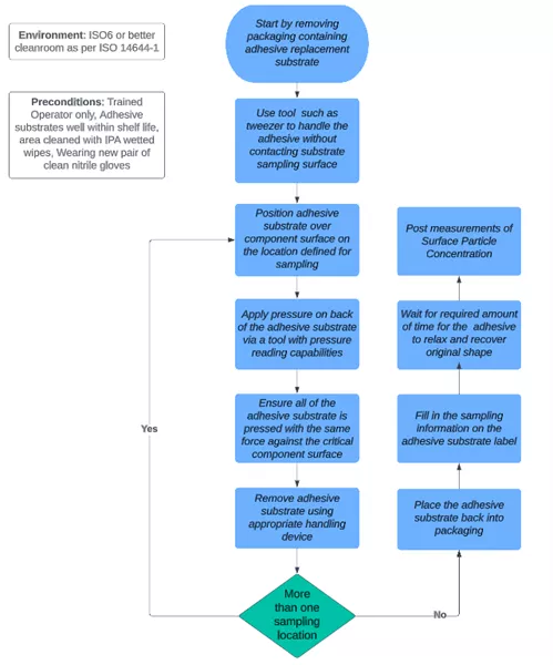
Test Method 2: Surface Contamination Measurement through Replacement Substrate and Optical Metrology
This test method describes the quantitative analysis method for measuring ISO 14644-9 surface cleanliness by particle concentration (SCP) of CCC using a replacement adhesive substrate to remove particles from the surface of interest and to measure them with a scatterometer, or scanning surface inspection system (SSIS), for particle counting, followed by a SEM/EDX analysis to identify the elemental composition of the particles.
Tape lifting via a clean adhesive replacement substrate has proven to be a valid alternative to direct inspection, where particles are removed from the surface of interest and transported directly to a measurement process. The methodology is described below after which calculations are performed to obtain the SCP and the reports are generated.
Fig 1. Test Method for Surface Contamination Measurement through Replacement Substrate and Optical Metrology
The SCIS Technology Community has been a hub for standards initiatives since its inception. It has published seven E and F series SEMI Standards since 2015, with three new standards currently in development. With the semiconductor equipment industry experiencing rapid growth, there has never been a better time to join SCIS. If you wish to get involved with SCIS activities, please contact Mayura Padmanabhan ([email protected]).
By implementing these advanced test methods, semiconductor wafer processing and inspection can achieve higher quality standards and enhance the reliability and yield of the resulting wafers and devices. The collaboration between suppliers and users, facilitated by standardized measurement methods, will further drive innovation and efficiency in the semiconductor industry.
Standards Watch
SEMI
www.semi.org
June 8, 2023