
Major Revision to Specification for Alphanumeric Marking of Silicon Wafers
By Kevin Nguyen, SEMI
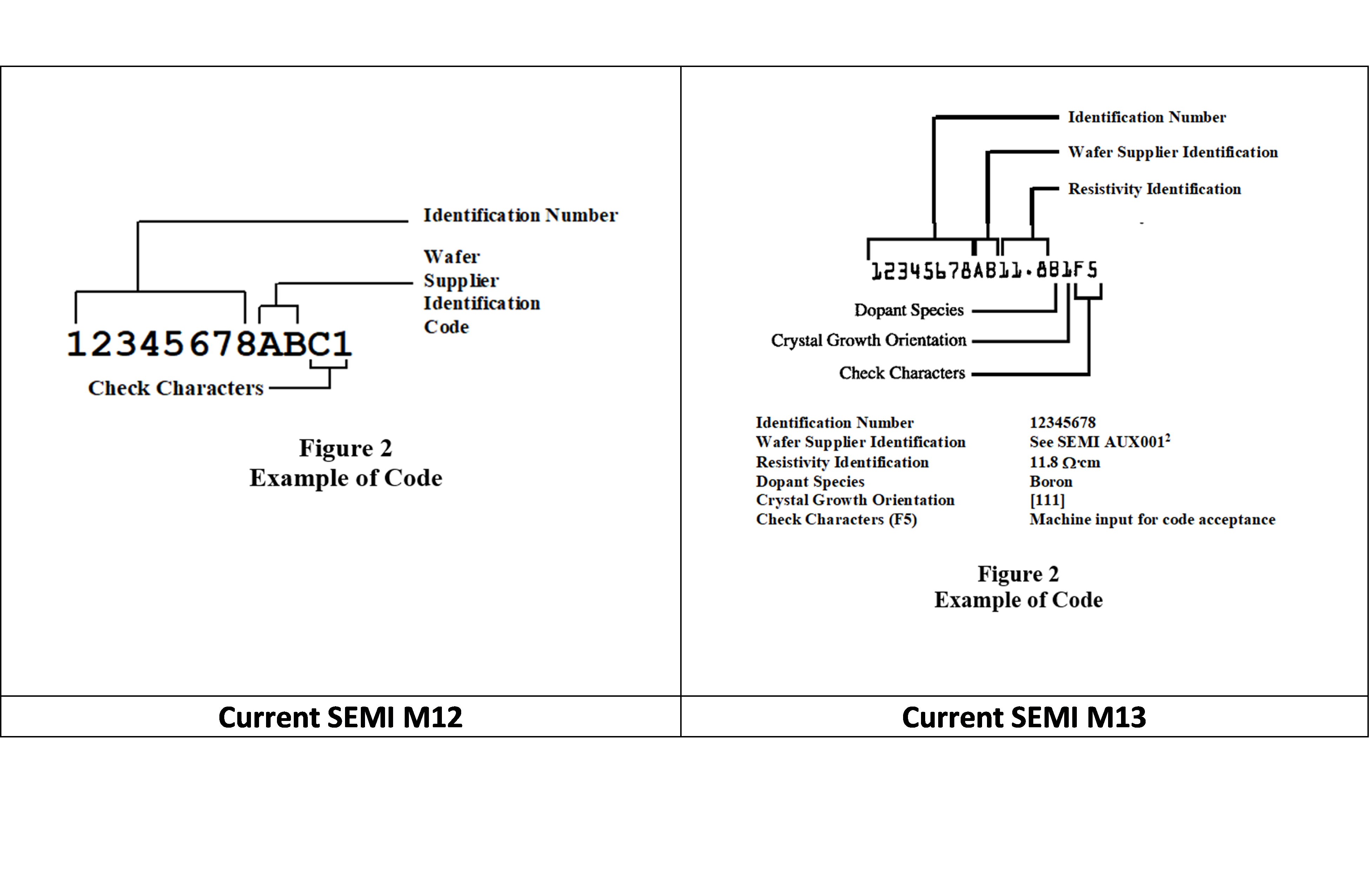
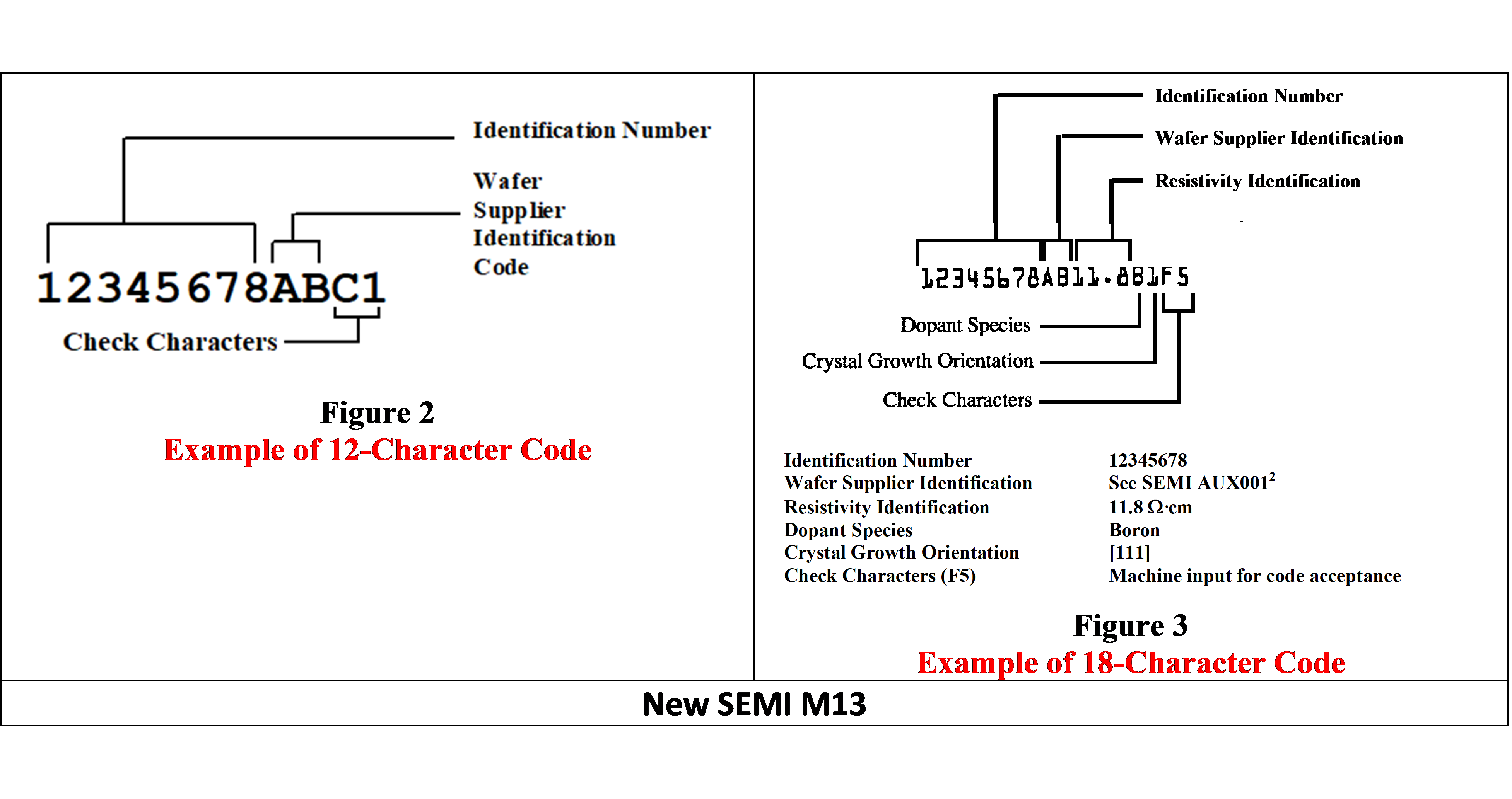
Laser markings on silicon wafers are an important part of the semiconductor fabrication to facilitate traceability of the manufacturing process. Initially published in 1989, SEMI M12 - Specification for Serial Alphanumeric Marking of the Front Surface of Wafers, specifies 12 character markings of silicon or other semiconductor flatted and notched wafers for 100 mm to 200 mm. In parallel, SEMI M13 - Specification for Alphanumeric Marking of Silicon Wafers, published in the same year, is almost identical to SEMI M12 but provides specification for 18 characters instead of 12. These two standards have significant overlapping contents including specification for character dimensions for height, width, thickness and spacing.
While these two legacy standards have been in existence since the late 90s, it is unclear to wafer suppliers and end users as to why there are two standards.
Led by Emily Liew, XFAB, the task force will eliminate confusion by clarifying the relationship of traceability standards and bring a common understanding of options available in the supply chain. The goal is to have a single standard that would cover wafer marking for 12 and 18 characters. The first order of business is to revise SEMI M13 (SNARF 6669) by consolidating all content of SEMI M12 into SEMI M13, as depicted in the figure below.
This effort is being carried out under the 5 Year Review Task Force (TF) under the supervision of the Traceability North America Technical Committee Chapter. Once Ballot 6669 (to be issued in Cycle 7-20) is approved and published, the TF will proceed with balloting withdrawal of SEMI M12. Subsequently, the TF will review related standards in the Materials volume (e.g., SEMI M1, M49, M67, and M68) and Traceability volumes (e.g., SEMI T7, T8, and T9) to identify those that reference SEMI M12 and update the references with SEMI M13.
To avoid surprises in the entire supply chain, all stakeholders need to weigh in. Ballot 6669 will be distributed to all members of the Global Silicon Wafer and Traceability Technical Committees.
Get Involved
SEMI Standards development activities take place throughout the year in all major manufacturing regions. To get involved, join the SEMI International Standards Program at: www.semi.org/standardsmembership. If you have any question about this activity, please contact Kevin Nguyen ([email protected]) or Michelle Sun ([email protected]).
Standards Watch
SEMI
www.semi.org
September 10, 2020