
SEMI Standards Roadmap for CMP Consumables Metrology
By Inna Skvortsova, SEMI HQ
SEMI will announce the release of the first Chemical Mechanical Planarization (CMP) Metrology suite of Standards for leading-edge semiconductor manufacturing at the upcoming Ultrapure Micro (UPM) conference taking place November 9-11, 2020 in Austin, Texas.
Supported by a co-moderating team of industry experts including Intel, Samsung Austin Semiconductor, and GLOBALFOUNDRIES, the UPM is annual event focused on micro contamination issues in the high purity environments of semiconductor manufacturing. Over the years the conference has expanded to address topics of ultrapure water, ultra-high-performance chemicals and high-purity gases as well as water management and wastewater treatment.
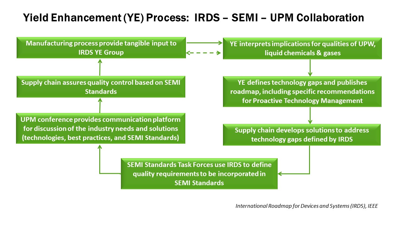
In 2020 the UPM program is bringing the discussion closer to the wafer, supporting the industry-wide efforts to enable yield by continuous process control improvements for advanced node IC manufacturing. This discussion will take place in the context of proactive technology management that requires tight collaboration among industry experts across various sectors of the supply chain. The following diagram describes the process currently used in the industry to define and address contamination issues constraining manufacturing yield:
One of the critical process modules for achieving sustainable yields in IC manufacturing is Chemical Mechanical Planarization (CMP) and post-CMP cleaning. This area is also one of the most difficult to control. "Any excursion in the CMP process is extremely expensive and can have a significant impact to device yields and device reliability. Multiple challenges, such as polishing hard materials (Silica) and soft materials (Cu) simultaneously while avoiding scratches and preventing corrosion of the surface, with ultimate goal of uniformity and global planarity of the processed wafer, are expected," states Don Hadder, Planar Process Engineer at Intel and Co-Chair of the North America Chapter of the SEMI Liquid Chemicals Technical Committee.
To ensure the variability is detected and then controlled, standardization of incoming supply chain parameters and standardized metrology for the CMP process is vital for the industry.
Driven by the growing complexity of the advanced semiconductor devices, industry experts representing Integrated Device Manufacturers (IDMs), CMP material suppliers, manufacturers of CMP distribution systems, and instrumentation manufacturers have joined efforts to develop the first suite of SEMI Standards focused on CMP consumables metrology. Specifically, these new standards will address critical CMP slurry and post-CMP measurements such as density, conductivity, pH, trace metals, particle counts, and abrasive particle size distribution, as well as CMP polishing pad hardness and density as a starting point with more parameters under consideration. The SEMI Standards Roadmap for CMP Consumables Metrology will be presented at the UPM 2020 conference High Purity Chemicals Session.
With time-to-yield being key to profitability, this new suite of SEMI Standards is expected to have a major impact on the industry by providing essential benchmarks for both industry suppliers and end-users. Achieving congruence in CMP suppliers’ specifications will allow IDMs to appropriately modify their processes to deliver optimal control of removal rates and reach consistency of the removals at the wafer surface.
Get Involved
If you have any questions regarding the SEMI Standards mentioned in this article or would like to participate in standards development, please contact Inna Skvortsova at [email protected] .
SEMI Standards development activities take place throughout the year in all major manufacturing regions. To get involved, join the SEMI International Standards Program at: www.semi.org/standardsmembership .
The next North America Liquid Chemicals Technical Committee Chapter Meeting is scheduled for March 31, 2020 in conjunction with the SEMI Standards North America Spring Meetings at SEMI Headquarters in Milpitas, California. To attend these meetings, you must be a SEMI Standards Program member . There is no cost, but registration is required .
Standards Watch
SEMI
www.semi.org
March 5, 2020