
From Silicon to Security
By James Amano, Senior Director, International Standards & EHS, SEMI
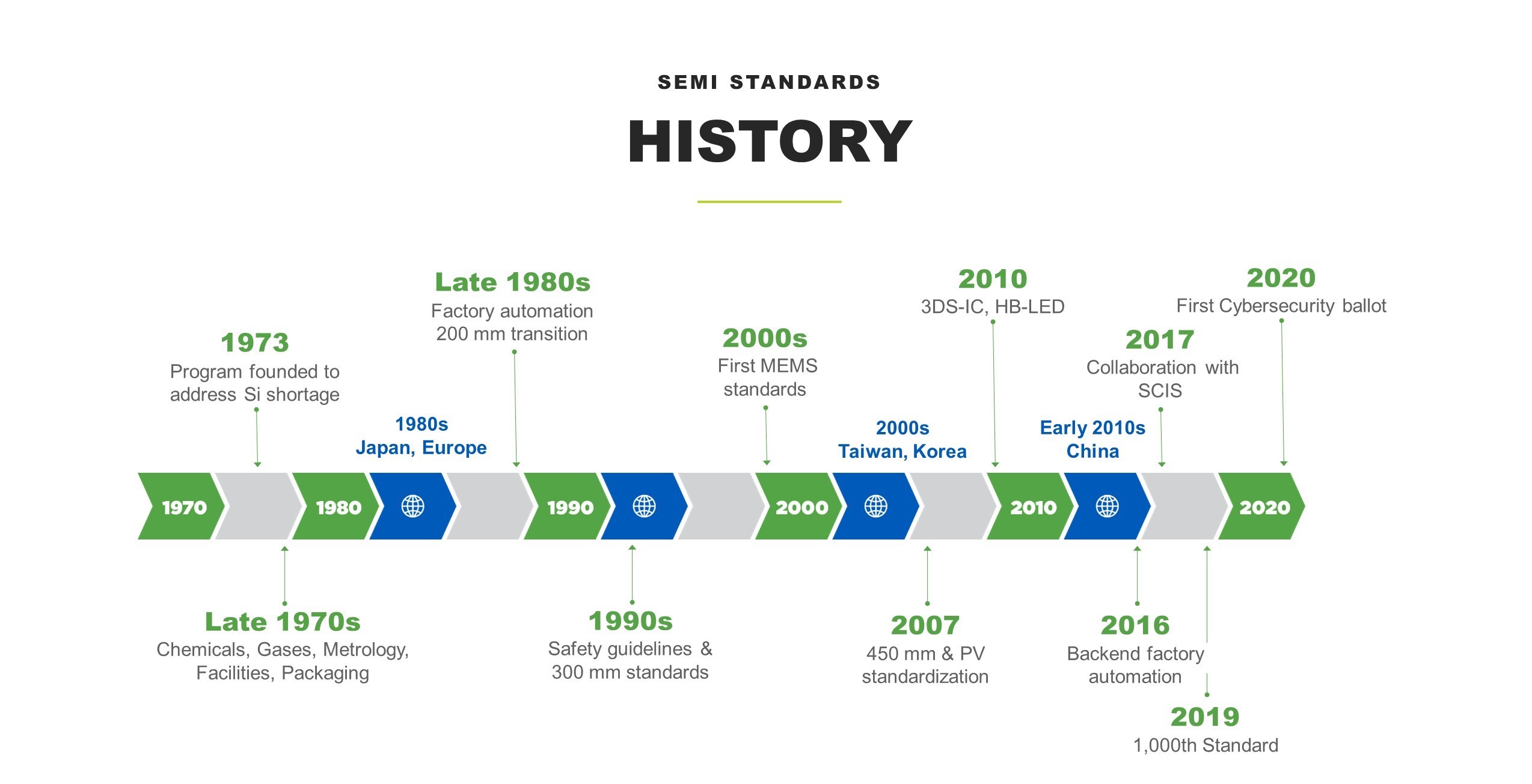
I’ve often written in the past on how the SEMI Standards Program continues to advance to meet the changing requirements of the industry, but it’s a topic worth returning to. While the Program initially focused on the electronics industry’s fundamental building block, the silicon wafer, things have progressed rapidly, particularly in the last few years, to the point where we’re now at work on industry-consensus Standards for cybersecurity.
When discussing the history of the Standards Program, progression can be (very) loosely grouped into substrates and materials; factory automation; safety; adjacent industries (display, photovoltaic, LED, etc.); and smart manufacturing. Previously, major standards efforts have been driven by wafer size transitions, but with the move to 450mm apparently on hold for now, what will be the next big topics that will have a big impact across the industry?
Some candidates include big data, artificial intelligence, quantum computing, power semiconductors, and sensors. As always, the Standards Program will rely on the collective intelligence of our members across the world to guide us forward.
The first 1,000 SEMI Standards in SEMI's first 50 years have driven down manufacturing costs and increased factory efficiency while improving worker safety, resulting in smaller, faster and smarter devices that have transformed the way we live and work. Committees are now active in China, Europe, Japan, Korea, North America, and Taiwan; if you aren’t involved yet, now is the time! SEMI Standards meetings are held throughout the year in all major manufacturing regions. For more information, contact your local Standards staff, and visit the SEMI Standards Web site.
Standards Watch
SEMI
www.semi.org
March 5, 2020