downloadGroupGroupnoun_press release_995423_000000 copyGroupnoun_Feed_96767_000000Group 19noun_pictures_1817522_000000Member company iconResource item iconStore item iconGroup 19Group 19noun_Photo_2085192_000000 Copynoun_presentation_2096081_000000Group 19Group Copy 7noun_webinar_692730_000000Path
Skip to main content
Default Banner Image

Tokyo Electron

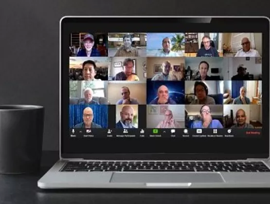
Tracking and quickly diagnosing COVID-19 infections, working from home and telemedicine recently came into sharp focus as technology executives and other subject matter experts from microelectronics heavyweights recently gathered for the first-ever virtual SEMI CTO Forum to explore how the microelectronics industry and their own companies can leverage future technology trends to drive growth. Themed Intelligent Medtech and Wearable Technologies, the forum drew CTOs from ARM, Babblelabs, Brewer Science, Dell, Dow/Dupont, E-Ink, Hewlett Packard Enterprise, Intel, Lam Research, KLA, Microchip, ON Semiconductor, Qualcomm, Tokyo Electron, Ulvac, Veeco and Xilinx. The event is designed as a strategic driver of pre-competitive innovation. Following are key takeaways from the forum. Microfluidics Promises to Speed COVID-19 Diagnosis More than 240 companies worldwide are developing microfluidics solutions to improve diagnosis and treatment of COVID-19 and other conditions, said forum speaker Dr. Kurt Petersen, a member of Band of Angels, Silicon Valley's oldest angel investment group, with an illustrious background1 in technology. And their innovations are bearing fruit. Cepheid, a company founded by Dr. Petersen, has developed a disposable microfluidic cartridge, Xpert Xpress SARS-CoV-2, used by doctors to swab the inside of a patient’s mouth. Highlighting the vital role of MEMS in medical electronics, the tiny powerful devices are behind a test that can detect COVID-19 infection in under 40 minutes. Dr. Petersen also cited a few examples of implantables and injectables under development, including: In vivo chemical sensing: Profusa developed a continuous glucose monitoring sensor via an optical patch. Glaucoma pressure monitors: Injectsense built a silicon chip the size of a grain of rice that is embedded in the eye to measure eye pressure. Retinal implants: Second Sight implanted a 60-electrode array chip that projects images onto the retina to improve vision. Microelectronics Takes Aim at Battling COVID-19 The event’s CTO roundtable, a platform for discussing societal and technology issues, revealed microelectronics technology will likely give rise to solutions for combatting pandemics and new business opportunities both in the short and long run. Areas of the greatest interest included: Tracking and Security: Infection tracking accuracy is key to limiting the spread of viruses yet comes with inherent privacy and security challenges. The consensus view of the executives was that developing trusted hardware capabilities is critical for adoption of accurate infection-tracking technologies. Remote Operation: Executives expect working from home or the use of telehealth to continue building momentum long after pandemic. To give staying power to the remote communications at the heart of these trends, microelectronics ecosystems will need to boost compute performance, both at the edge and in the cloud, while increasing bandwidth to enable applications such as augmented reality/virtual reality (AR/VR), artificial intelligence (AI), machine learning and advanced data analytics. Edge intelligence: The challenge of remote communications spans both people and the Internet of Things (IoT). Questions persist about how hundreds of billions of sensors will connect to the cloud and how much power they will consume. The need to push computing to where data is generated – at the edge – is rising and the necessary underlying technologies will only come by combining various forms of distributed computing and analytics. The microelectronics industry’s ability to seize these opportunities will only be possible with huge strides in innovation, raising concerns among the CTOs about the financial viability of cutting-edge devices because of increasing device complexity and R D costs. Technology partnerships and collaborations – an area where SEMI is contributing and will continue to expand its efforts as it works with the CTO community – will be critical to containing R D costs. SEMI will help the executives identify and mobilize the resources key to future innovation. Improving Home, Work Productivity and Experiences Key to AR Adoption Smart wearables also offer great promise. In just over a decade, AR and VR have grown from science fiction to practical uses such as AR applications for smart contact lenses, said Dr. Mike Wiemer, Co-Founder and CTO of Mojo Vision2. Dr. Wiemer said that while many AR applications remain under development, the technology will only see widespread adoption once it starts to improve productivity and efficiency at home and work and the quality of other experiences. The smart augmented reality contact lens developed by Mojo Vision is a step in that direction. The product’s built-in display gives users timely information about everything they see while remaining invisible by packing 70,000 pixels into a space smaller than a half a millimeter across, making it the smallest and densest dynamic display ever made. The contact lens is powered by an ARM-based processor, with later versions adding an image sensor, eye-tracking sensors and a communications chip. SEMI thanks EMD Performance Materials and Telit for sponsoring the CTO Forum. For more information on the CTO Forum and SEMI’s Smart Data-AI initiative, please sign up on our webpage. 1 Dr. Kurt Petersen is a member of the National Academy of Engineering, an IEEE Medal of Honor winner, and a Life Fellow of the IEEE for his contributions to the commercialization of MEMS technology. 2 Dr. Wiemer also co-founded Solar Junction, where he led technical teams to two world records in solar cell efficiency (43.5% and 44%). He also has patents and papers in Semiconductor Devices Applications, Silicon Photonics, Materials Integration, Lasers, Solar Cells, Solar Systems, and Analog Circuits. Tom Salmon is Vice President of Collaborative Technology Platforms at SEMI. Pushkar P. Apte, Ph.D., is Strategic Technology Advisor for the Smart Data AI Initiative at SEMI.
Read More
Once an unpopular career destination for university graduates in Korea, the semiconductor industry has been a plum target since the rise of Samsung Electronics and SK Hynix as global leaders and key growth engines for the Korean economy. The industry’s outsize role in innovation of cutting-edge technologies and applications such as artificial intelligence (AI), Internet of Things (IoT), 5G and autonomous driving has added to the appeal.The draw of a career in chip manufacturing is even stronger when new graduates from Korean universities consider the semiconductor industry’s rapid growth of 22.2% in 2017 and 15.5% in 2018, according to VLSI Research. Yet, even before earning their degrees, many students are unclear about steps they need to take to prepare for a career in the industry and the type of work available to them.These questions and concerns were on the top of the minds of 250 students who gathered at COEX in Seoul in mid-November for SEMI Campus Outreach, a half day of career insights from global chip companies including Lam Research, Applied Materials, Tokyo Electron, and KLA along with leading semiconductor companies in Korea such as SEMES, EO technics, JUSUNG ENGINEERING, DONGJIN SEMICHEM, PSK and Wonik IPS. Keynote - Inhak Harry Suh, CEO, Lam Research Korea 250 students gathered at Campus Outreach Campus Outreach keynote speaker Inhak Harry Suh, CEO of Lam Research Korea, stressed that talented new graduates hold the key to leading the semiconductor industry into the Industry 4.0 era and the next phase of growth. He urged the students to look for a company that treats its employees with respect and fairness and to enjoy their work. Joining the executives in inspiring the students, field and service engineers highlighted the semiconductor industry’s strong growth potential, described their job responsibilities and the skills students need to develop to thrive, and offered guidance on subjects to study in school to best prepare students for jobs in the industry. On the recruiting side, human resources representatives at the event provided overviews of their companies and skills they’re looking for as they court talent. Campus Outreach sponsors At SEMICON Korea 2020 – Feb. 5-7 at COEX in Seoul – SEMI will continue to cultivate industry talent at the Workforce Development Pavilion. To help the industry solve its critical talent shortage, the pavilion will offer university students interviews with industry experts and tutorials on semiconductor production as the students explore career paths and are mentored by engineers during the Meet the Experts program. And with a diverse workforce recognized as a competitive advantage, the Women-in-Technology session will gather leaders to discuss how the industry can improve diversity.Jaegwan Shim is a marketing specialist at SEMI Korea.
Read More
Famous for its warmth and hospitality, Japan always welcomes visitors from around the world with a gracious embrace. But when is the best season to visit? It depends on the interest of each visitor of course. For Instagrammers, the April cherry blossoms or November autumn leaves – a masterpiece of art with their rainbow gold, red and yellow hues – are ideal for snapping memorable pictures. For foodies, winter delights with tuna, toro sushi and other seafood at their tastiest. Wagyu peaks in richness, too, when the cold weather sets in. For anime and manga enthusiasts, August is definitely the time to visit. That’s when COMIKET, the world’s largest comic market – drawing more than a half million people – takes place in Tokyo. But for people in the electronics value chain, the perfect time to pack their bags and hop a flight to Tokyo is December, when SEMICON Japan – December 11-13 at Tokyo Big Sight – opens its doors with its own form of hospitality.Why should you attend? Here are the five top reasons.Reason 1: Japan is home to leading electronics industry suppliersAccording to VLSI Technology, seven of the top 15 semiconductor equipment suppliers in 2018 are headquartered in Japan, and many Japanese companies also lead backend equipment segments. For decades, Japanese companies have supplied about one third of the equipment for the global semiconductor equipment industry, according to SEMI and the Semiconductor Equipment Association of Japan (SEAJ). Most of these companies typically set up a booth on the SEMICON Japan show floor to welcome your visit.True, many Japanese suppliers also exhibit at SEMICON shows outside of Japan to meet with customers. But you will find many more engineers, managers and executives of equipment suppliers on their home ground at SEMICON Japan, where suppliers typically debut new equipment. Their booths are also ideal locations for visitors to meet with suppliers to ask questions, exchange opinions and negotiate new business deals.Japanese materials suppliers enjoy an even larger market share, providing about half the materials for the global semiconductor industry. These suppliers dominate in silicon wafers, photomasks, photoresists, sputtering targets, packaging substrates, bonding wires, leadframes, mold compounds and wafer level packaging dielectrics. Unlike equipment suppliers, not all materials companies exhibit. Instead, many participate as speakers and attend to connect with customers.Reason 2: Get ready for the next semiconductor industry upturnA year ago, in late 2018, we expected chip inventory to stabilize by mid-2019, yet the industry still struggles with high inventory overall and low average selling price for memory. The SEMI 2019 equipment billing forecast was lowered accordingly from -4.0 percent growth (2018 year-end forecast) to -18.4 percent (2019 mid-year forecast). However, the two forecasts still predict positive growth in 2020. As SEMICON Japan 2019 is underway, we should be at the beginning of the next upturn.The chart below shows that more wafer process fabs will start construction in 2020 than this year. (Please see article: Nearly $50 Billion in Fabs to Start Construction in 2020.) Custer Consulting Group also pointed to “a resumption in semiconductor chip and capital equipment growth in late 2019 or early 2020.” (Please see article: Semiconductor Industry Upturn by Early 2020?.)With better times ahead, SEMICON Japan 2019 will be an opportune time to exchange opinions with key players across the supply chain and start negotiations for the coming robust recovery of the equipment, components and materials markets.Reason 3: Glimpse the future at SuperTHEATERSEMICON Japan SuperTHEATER will feature industry and technology insights from global visionaries. Asako Eda, Japan’s chief representative officer of the World Economic Forum and the former president of Intel Japan, will open the SuperTHEATER with her keynote on how we live in an era where the fourth industrial revolution, climate change, disparity and geopolitical risks are affecting our lives and with the speed we have never experienced. She will explore the growing role of innovation and social responsibility and how the World Economic Forum is addressing associated challenges. The opening keynote session will also feature Nandan Nayampally, vice president and general manager of the Immersive Experience group at Arm.In all, the SuperTHEATER will host seven keynote forums over three days at SEMICON Japan including: Semiconductor Executive Forum – Terushi Shimizu, representative director and president of Sony Semiconductor Solutions, and Atsuyoshi Koike, president of Western Digital Japan, will discuss their business strategies and prospects. Manufacturing Innovation Summit – Executives from Applied Materials, KLA, Nikon and Tokyo Electron will discuss business and technology issues as well as innovations that will drive growth to 2030. All seven SuperTHEATER programs will be simultaneously translated to English for international audiences.Reason 4: Connect to application communitiesCollaboration across the value chain has never been more important to industry innovation and growth – the very reason SEMI has expanded its reach beyond the semiconductor manufacturing supply chain (equipment and materials) to include design, systems and products.The SEMICON Japan show and conferences will connect you to key application segments of the value chain. The SuperTHEATER will host two SMART transportation forums highlighting the latest developments in autonomous driving and sky transportation (flying cars). In the SMART Applications Zone on the show floor, you’ll find electronics products and technologies showcased for automotive and manufacturing automation as the autonomous driving pavilion highlights emerging technologies that are driving semiconductor innovation opportunities. Reason 5: Learn from disaster and recovery experiencesJapan has taken important disaster recovery lessons from devastating earthquakes over the past three decades, most notably the Kumamoto quake in 2016, the Tohoku temblor in 2011 and the Kobe rattler in 1995. So has the Japan electronics supply chain, including SEMI members. In the Business Continuity Plan (BCP) area at SEMICON Japan 2019, exhibitors including DISCO, Murata Machinery and THK will highlight technologies that can strengthen your preparedness for a disaster and aid in the recovery.On December 12 at the BCP seminar at Japan 2019, Sony Semiconductor Manufacturing, DISCO and Team Engineering Consulting will share their experiences and expertise in mitigating the disaster impacts. (Sony and Disco will present in Japanese.)To get the feel for the magnitude of a major earthquake and how seismic isolation protects against structural damage, be sure to take advantage of THK’s earthquake experience car. Seismic isolation installs isolators – rubber bearings, friction bearings, ball bearings, spring systems or other devices – beneath a building to buffer earthquake vibrations transmitted to structures.More reasons to attend SEMICON JapanAnd of course your visit to Tokyo for SEMICON Japan 2019 wouldn’t be complete without exploring Tokyo and other regions to experience Japan’s exotic culture, cityscapes and cuisine! Here are some resources to give you even more reasons to book a flight to Tokyo: Japan National Tourism Organization Go Tokyo Kyoto Tourism I look forward to seeing you at SEMICON Japan in December!Jim Hamajima is president of SEMI Japan.
Read More
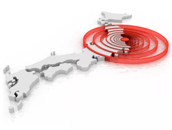
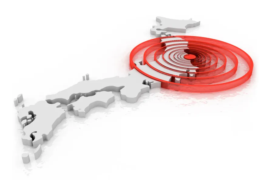
Wedged among four major tectonic plates, Japan is at the mercy of their abrupt herculean shifts and the earthquakes and tsunamis they can trigger. The fallout can be devastating. The magnitude 9 Great East Japan (Tohoku) temblor in 2011 and ensuing tsunami took nearly 20,000 lives, destroyed 138,000 buildings and cost $360 billion in economic damage.Factories including silicon wafer production facilities owned by Shin-Etsu Chemical and MEMC Electronic Materials – together accounting for 25 percent of the global silicon wafer production – sustained heavy damage. Operations were suspended. The Kumamoto earthquake in 2016 also caused significant damage. The economic cost: as much as $7.5 billion.With disaster risk rising on a global scale, these calamities offer valuable lessons in disaster preparedness and how companies can draw from their experiences to strengthen business continuity planning (BCP).Earthquake experiences and lessons in BCP were the focus of the recent SEMI Japan Members Day as speakers from five semiconductor device and equipment manufacturers offered their BCP strategies to about 150 SEMI members. Following are key takeaways from their presentations. Renesas: Create a robust production plant that is hard to break and easy to fixRenesas Semiconductor Manufacturing’s Naka plant took about 80 days to resume production while its ability to deliver semiconductors was delayed even longer as it recovered from damage caused by the Tohoku earthquake, said Yoshiyuki Miyamoto, Representative Director and President at Renesas. Operations at the company’s Kawajiri plant were disrupted by the Kumamoto earthquake.A key lesson from both earthquakes: The company needed to promote risk visualization from top-to-bottom in the supply chain. With the goal of making its plants easy to repair but hard to break down, Renesas implemented a risk management plan for earthquake preparedness plan to ensure stronger production line resistance and a stable supply to customers. The company ran simulations of multiple earthquake scenarios including aftershocks, enabling it to develop new BCP training and preparedness measures. Sony: Staying transparent about the disaster, sharing and interacting with related companiesYukihide Keigo, a representative from the Sony Semiconductor Manufacturing, showed footage taken the day the Kumamoto earthquake damaged a production line at its Kumamoto Technology Center. Sony is the top manufacturer of imaging sensors worldwide, and the Kumamoto plant is the backbone of that production. The magnitude of the foreshock fell within levels Sony had accounted for in its BCP at that time, and the line was expected to return to full production within a week. However, the magnitude of the earthquake that followed outstripped expectations, and the company’s BCP didn’t hold up. Three and a half months later, the plant had finally fully recovered. The protracted recovery prompted Sony to develop an earthquake preparedness plan using a model that assumed double the magnitude of expectations. For full restoration, the company identified challenges to returning to full operation at each stage of the production line. Then it went even further, developing in-house diagnostics, implementing critical path methods and strengthening earthquake resistance of equipment that manages bottlenecks for the restart of the plant. The revision of its BCP plan led to the establishment of a system to shorten the resumption of production after a major earthquake to just two months.Sony shared the contents of its BCP review with other companies to solicit help identifying any gaps and highlighted its partnership with Renesas in the Semiconductor Industry Association in Japan (JSIA), a committee of the Japan Electronics and Information Technology Industries Association (JEITA), to share materials procurement resources for the purposes of disaster preparedness and business continuity. HORIBA STEC: Steady daily practices protect hundreds of millions of yen worth of products HORIBA STEC’s Aso plant, near the epicenter of the Kumamoto earthquake, suffered heavy damage that cut off electricity and the water supply, yet production in its clean room resumed in just 10 days, said Hiroyuki Koyama, a factory manager at the plant. The plant’s quick recovery stemmed from daily preventive measures implemented before the quake such as connecting freestanding shelves for greater stability, applying thick rubber bands as rails to prevent manufactured goods from falling to the floor, and placing equipment on rolling carriages instead of fixed shelves.The practices saved the Aso plant hundreds of millions of yen in products and materials that otherwise could have been lost in the earthquake. Koyama also offered the reminder that, with regulations governing factory layout and construction differing widely depending on factors such as a building’s age, companies need to tailor their BCPs to the unique characteristics of each building. THK: The key point of dampening earthquakesTHK’s ACE Division develops earthquake dampening and vibration control devices designed to absorb the vibrational energy of an earthquake, though the devices must also be designed for precise analysis of that energy, said Hidemi Murao. Murao provided an overview of the latest technologies and products for dampening earthquake vibrations and shared test results from experimental devices.Murao described how THK’s recently introduced Linear Motion (LM) Guide, an earthquake vibration dampening technology, can significantly reduce building vibrations during a temblor. In a video Murao showed to demonstrate how the guide works, a shelf loaded with equipment rests on a platform equipped with THK’s LM Guide equipment. Simulating an earthquake, the platform shakes vigorously in every direction but the shelf remains steady as the LM Guide dampens the vibrations. The platforms can be installed on floors or underground in buildings or factories to prevent shelves from toppling. Tokyo Electron: The ideal BCP management systemOne risk associated with BCP training is that it can become overly routine, dulling the response of employees in actual disasters, said Tokyo Electron Vice President Tatsuya Aso. To help keep its workers’ skills sharp, TEL held surprise drills with employees assigned to particular BCP roles to test their ability to adapt quickly to when disaster strikes. In addition, TEL has launched surveys in more than 70 overseas locations to optimize safety in these high-hazard facilities.The SEMI Japan Members Day presentations made clear that the issue of BCP transcends boundaries between individuals, manufacturers, regions, and sectors within the global electronics supply chain. Disaster preparedness requires problem-solving across the entire supply chain, with companies sharing technical knowledge, offering mutual aid, and striving for continual improvement. Collaborative is essential. At SEMICON Japan 2019, SEMI will continue to bring companies together to address BCP initiatives and share their technical knowledge with members. Jim Hamajima is president of SEMI Japan.

Read More