downloadGroupGroupnoun_press release_995423_000000 copyGroupnoun_Feed_96767_000000Group 19noun_pictures_1817522_000000Member company iconResource item iconStore item iconGroup 19Group 19noun_Photo_2085192_000000 Copynoun_presentation_2096081_000000Group 19Group Copy 7noun_webinar_692730_000000Path
Skip to main content
Default Banner Image

memory

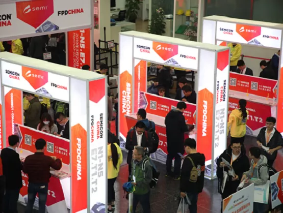
For the second straight year, SEMICON China, among the world’s largest and most influential semiconductor industry events, was the first local tradeshow of its scale held in-person, reflecting China’s rising prominence in the semiconductor industry. After securing approval from the Chinese government to hold large events, SEMI staged SEMICON China 2020 and 2021 with advanced protections against COVID-19 in place. There were no reported infections at either event. Highlights from SEMICON China 2021: Large Scale: Attendance of over 92,000, including more than 66,000 visitors and 25,000 exhibitors. Expo hall totaled 84,500 square meters with about 1,100 exhibiting companies and over 4,000 booths. World-Class Thought Leaders: Strong industry support from key foundries, OSATs, equipment and materials suppliers. Keynote speeches featured world-class industry leaders and head of China’s IC industry fund and global investment consulting agency, who explored the latest global business, technology and market trends and hot domestic investment topics. Concurrent Forums: Forums included SIIP China: SEMI Innovation Investment; Smart Manufacturing; Advanced Manufacturing; Advanced Packaging; Memory; Power Compound Semiconductor; China Display Conference; the all-new Advanced Materials Forum; and China Semiconductor Technology International Conference (CSTIC). Rich Digital Content: SEMICON China’s digital platform provided a rich array of content to attendees around the world including the Grand Opening Keynote and CSTIC, which were broadcast live online. Workforce Development: SEMI China worked closely with industry and government partners to promote SEMI Workforce Development programs to help attract and retain talent for China’s semiconductor industry. SEMICON China again featured the SEMI Workforce Pavilion and SEMI Workforce CXO Talent Forum. Outstanding COVID-19 Protective Measures: SEMICON China deployed advanced testing and monitoring equipment and implemented strict COVID-19 preventative measures to ensure a safe environment for all attendees to network and conduct business. Looking Ahead With the resounding success of SEMICON China 2021, optimism is growing that more physical events will be held with travel restrictions set to ease later this year. The more than 2,500 SEMI members around the world are eager to again network and collaborate face-to-face with customers, suppliers and partners to solve challenges in the microelectronics industry and drive semiconductor innovation that continues to transform how we work and live. That very innovation made many businesses more resilient as the virus spread and enabled people worldwide to work, learn, and shop from home. As SEMI starts to stage other events in-person, we will put in place advanced protective measures against COVID-19 to ensure the safety and well-being of all attendees. As the vaccination roll-out continues worldwide and new COVID-19 strains emerge, SEMI’s flagship SEMICON events are evolving in several ways, most notably with a larger digital presence. In this new era, we offer an international platform for SEMI members and partners across the microelectronics supply chain to collaborate, discuss industry trends, solve common challenges, network, and accelerate business growth through physical, virtual, and hybrid formats. Hybrid events – on-site exhibitions and conferences featuring a digital presence – allow the face-to-face connections so important to the semiconductor industry but also improve the attendee experience by offering an online option with the following benefits: More international accessibility to content live or on-demand Robust interactivity with live-streamed events, allowing more people to participate Greater cost effectiveness to enable companies and people under tight budgets to take advantage of world-class content, including keynote presentations, panel discussions, and technical sessions. In a recent survey of advanced manufacturing businesses, Informa Markets, a multinational publishing, business intelligence, and exhibitions group, found that 93% of respondents are likely to return to in-person events between August and December 2021, signaling a widespread eagerness for the return of live events and face-to-face connections. SEMICONs Scheduled for 2021 In a normal year, each of the seven regions where SEMI operates stages a SEMICON, with the exhibitions spread throughout the year. With the world continuing to combat COVID-19, more SEMICONs have been moved to the second half of 2021 – most of them with a hybrid format so exhibitors and attendees can take advantage of the increasing popularity of online events. After last year’s disruptions to the SEMICON schedule – and with more experience in the new normal – SEMI is excited to welcome the businesses and peers who couldn’t attend the 2020 events back to the in-person and hybrid shows. Innovation never sleeps. And SEMI will continue to evolve its events to help you form the partnerships and make the connections vital to the growth of your company and the industry. For more information about regional SEMICONs, please visit the SEMI events page. About the Author David Ghodsizadeh is the Director of Global Product Marketing at SEMI, where he develops customer-centric strategies to market SEMI Membership, Market Data, Expositions, Smart Initiatives, and Technology Communities to members, partners, and industry peers. Connect with David on LinkedIn.
Read More
In the long unfolding arc of technology innovation, artificial intelligence (AI) looms immense. In its quest to mimic human behavior, the technology touches energy, agriculture, manufacturing, logistics, healthcare, construction, transportation and nearly every other imaginable industry – a defining role that promises to fast track the fourth Industrial Revolution. And if the industry oracles have it right, AI growth will be nothing shy of explosive.“The gains these days are not incremental,” said Ajit Manocha, SEMI president and CEO, said to a gathering in July of the Chinese American Semiconductor Professional Association (CASPA) for its Summer Symposium at SEMI’s headquarters in Milpitas. “They are hockey stick – exponential – with AI semiconductors growing in market size from $4 billion this year to $70 billion in 2025.”Manocha left little doubt that AI is remaking the semiconductor industry and, in the process, the world at large. Internet of Things (IoT) and 4G/5G, both key AI enablers, will account for more than 75 percent of device connections by 2025.“Today, 30 billion devices worldwide are connected,” Manocha said, citing an Applied Materials prediction that the number of connected devices globally will grow to between 500 billion and 1 trillion by 2030. Those devices will generate stunning amounts of data collected, interpreted and used to reason, solve problems, learn and plan, leading to the holy grail of autonomous machine behavior.To process this colossal amount of data central to the promise of AI, the industry must break through the limits of a key technology: memory. Memory a Critical AI BottleneckThe challenge for memory starts with performance. Historically, every decade gains in compute performance have outpaced improvements in memory speed by 100 times, and over the past 20 years that gap has grown, said Steven Woo, a fellow and distinguished inventor at Rambus, presenting at the symposium. The upshot is that memory has bottlenecked compute and, in turn, AI performance. The industry has responded with new ways to implement memory systems on AI chips. Each is suited to unique performance requirements and, of course, comes with trade-offs. Among the frontrunners: On-chip memory delivers the highest bandwidth and power efficiency but is limited in capacity. HBM (High Bandwidth Memory) offers both very high memory bandwidth and density. GDDR balances trade-offs among bandwidth, power efficiency, cost and reliability. Since 2012, AI training capability has grown 300,000 times, besting Moore’s law by 25,000 times in doubling every 3.5 months, a blistering pace compared to the 18-month doubling cycle of Moore’s law, Woo said. The staggering improvements have been driven by parallel computing capacity and new application-specific silicon like Google’s Tensor Processing Unit (TPU).These specialized silicon architectures and parallel engines are key to sustaining future gains in compute performance and combatting the slowing of Moore’s Law and the end of power scaling, Woo said. By rethinking the way processors are architected for certain markets, chipmakers can develop dedicated hardware capable of operating with 100 to 1,000 times greater energy efficiency than general purpose processors to overcome another big limiter to scaling compute performance – power.For its part, the memory industry can improve performance by signaling at higher data rates and using stacked architectures like HBM for greater power efficiency and performance, and by bringing compute closer to the data.Memory scaling for AIA key challenge is scaling memory for AI. Demand for better voice, gesture and facial recognition experiences and more immersive virtual reality and augmented reality interactions is tremendous, said Bill En, senior director at AMD, speaking at the symposium. These capabilities require more processing power across both high-performance computing (HPC) for big data analytics and machine learning as it relies on AI and machine intelligence to generate meaningful insights. Emerging machine learning applications include classification and security, medicine, advanced driver assistance, human-aided design, real-time analytics and industrial automation. And with 75 billion IoT-connected devices – all generating data – expected by 2025, there will be no shortage of data to analyze, En said. The wings alone of a new Airbus A380-1000 feature some 10,000 sensors.Mountains of this data are stored in massive data centers on magnetic hard drives, then transferred to DRAM before moving to SRAM within the CPU for the handoff to the compute hardware for analysis.With data growing at an exponential clip, the question is how to make sure all other memory systems can handle the flood of data. AMD’s answer is a chiplet architecture featuring eight smaller chips around the edge that drive the compute and a large chip in the center that doubles the IO interface and memory capability to in turn double chip bandwidth.AMD has also moved from a legacy GDDR5 memory chip configuration to HBM to bring memory bandwidth closer to the GPU for more efficient processing of AI applications. The HBM provides much higher bandwidth while reducing power consumption. Compared to DRAM, AMD’s HBM delivers a much faster data rate and far greater memory density, En said.Over the next decade, look for more performance improvements from multi-chip architectures, innovations in memory technology and integration, aggressive 3D stacking and streamlined system-level interconnects, he said. The industry will also continue to drive performance gains in devices, compute density and power through technology scaling.Michael Hall is a global marketing communications manager at SEMI.
Read More
We are living in a digital world where semiconductors are taken for granted, AI is bringing semiconductors back into the deserved spotlight, and now we are witnessing the dawn of the Cognitive Era enabled by semiconductors,” SEMI president and CEO Ajit Manocha said to an audience of more than 500 during his presentation – Rebirth of the Semiconductor Industry – at the First Global IC Entrepreneur Conference.Speaking at the Shanghai event in mid-December, Manocha recalled how, when he first entered the semiconductor industry in the 1980s, semiconductors revenue topped out at about $10 billion. Now, with sales having swelled to a staggering $450 billion, the industry is on a much faster growth track. Revenue could reach $500 billion by the end of 2020 and trillions of dollars by 2030. Over the past two decades, chips have given rise to social media and e-commerce powerhouses such as Google, Facebook, and Alibaba. All rely on heavily on chips, the engines of data centers across all industries. Wave after wave of technology innovation have been powered by semiconductors – from mainframe computers in the 1970s, personal computers in the 1980s, the Internet in the 1990s, and mobile and social networking in the early 20th century, to the current shining stars of technology such as IoT, big data, new memory, virtual reality, autonomous driving and artificial intelligence, Manocha said. New applications across areas such as smart manufacturing and digital healthcare are stoking the latest round of semiconductor growth.The rise of AI, like all the technologies before it, has renewed the semiconductor industry once again with its promise to drive growth of all industries worldwide, Manocha said. Five years ago, IoT was but a gleam in a technologist’s eye, more hype than reality with doubt about its viability running deep. Today, with about 60 percent of people in the world connected to the Internet, the enormous promise and potential of IoT is flowering. Industry growth will explode as the melding of AI and IoT birth countless applications and innovations in SMART transportation (0 emissions; 0 fatalities; 0 congestion), smart sensors (agriculture, infrastructure, healthcare) and SMART “Everything” (people, devices, homes, cities, industries, and the list goes on). Indeed, AI is now widely recognized as a chief growth driver of the semiconductor industry well into the future, with semiconductor technology at the core of AI innovation, he said. Semiconductors are thrusting the fifth industrial revolution into the fast lane. China’s much-anticipated rise as an industry powerhouse over the next few years will only accelerate industry growth, turning current disruptions into future opportunities as SEMI China continues to cultivate connection, collaboration and innovation in China’s fast-growing semiconductor sector.Cherry Sun is a marketing manager at SEMI China.
Read More
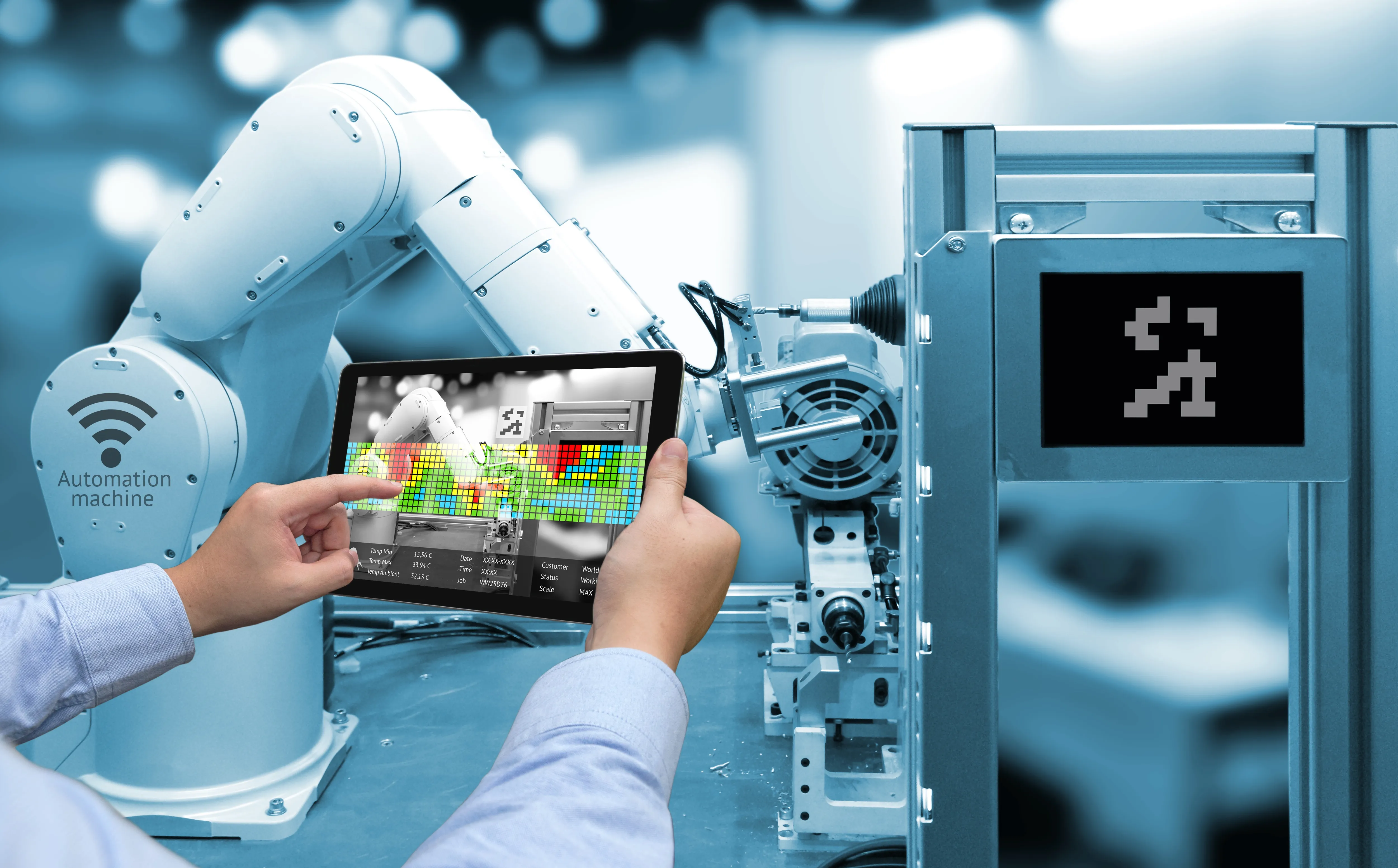
The march to greater precision, efficiency and safety – the lifeblood of high-technology manufacturing facilities – has taken on a new urgency as emerging applications such artificial intelligence (AI), the Internet of Things (IoT) and Industry 4.0 give new meaning to smart factories. Facing fiercer competition and ever more sophisticated fabrication processes, semiconductor fabs are under intense pressure to keep pace with new technologies as they work to upgrade. Nowhere are the stakes higher than in Taiwan, where high-tech manufacturing contributes mightily to the region’s GDP growth. To help Taiwan fabs confront the challenges and opportunities of designing smarter factories, SEMI and its High-Tech Facility Committee hosted the High-Tech Facility Workshop in June. SEMICON Taiwan 2018 High-Tech Facility Pavilion exhibitors gathered to explore how they can build smarter factories by deploying smart surveillance and disaster prevention technologies along with smart communications systems that better use manufacturing data to drive new safety and product quality efficiencies.During the workshop, SEMI High-Tech Facility Committee representatives shared strides it has made upgrading overseas facilities and developing standards to help establish smart factories in Taiwan.SEMICON Taiwan – 5-7 September at Taipei’s Nangang Exhibition Center – is also an important event for advancing smart manufacturing in Taiwan. Nearly 30 leading global manufacturers will exhibit at the SEMICON Taiwan High-Tech Facility Pavilion. The venue covers operational aspects of semiconductor manufacturing vital to becoming smarter including energy savings, nano-contamination control, facility information modeling, precision instrumentation and control, fire protection, mechatronics, and automation control. The pavilion will also feature a series of theme events offering a comprehensive overview of topics including the latest practices for integrating smart facility capabilities from the perspective of an advanced fab designer.At the TechXPOT stage, High-Tech Facility Pavilion exhibitors will also demonstrate the latest technology breakthroughs and cutting-edge smart factor solutions.The September 6th High-Tech Facility International Forum at SEMICON Taiwan will again gather factory experts and thought leaders from industry and academia to examine “Effective Ways to Make a Facility Smart.“ Experts from industry heavyweights in the fields of wafer foundry, LCD, memory and semiconductor packaging including TSMC, UMC, Innolux, ASE, Micron Taiwan, Winbond and VIS will offer insights into key areas of high-tech facilities including facility electricity, machinery, water management, vaporization and automation systems. On the same day as the forum, the High-Tech Facility Get-Together and High-Tech Facility VIP Dinner will bring together industry elites, academic professionals, and government officials to explore partnership opportunities. SEMI Taiwan and the High-Tech Facility Committee share HTF market trends information, technology updates and standards with SEMI members and exhibitors. Founded in 2013, the High-Tech Facility Committee now has 85 corporate members. Dedicated to accelerating industry collaboration through the integration of Taiwan industrial, government and academic resources, the committee each year holds several group meetings focusing on topics including energy savings, earthquake and fire protection, nano-contamination control, and precision instrumentation and control to advance critical technologies and facilitate standardization. The committee also aims to help the industry become more competitive faster by promoting technology standards that boost productivity and reduce production costs.Please visit www.semi.org and www.semicontaiwan.org for more information about SEMI’s high-tech facility initiatives.Iris Tsou is a marketing specialist at SEMI Taiwan.
Read More