downloadGroupGroupnoun_press release_995423_000000 copyGroupnoun_Feed_96767_000000Group 19noun_pictures_1817522_000000Member company iconResource item iconStore item iconGroup 19Group 19noun_Photo_2085192_000000 Copynoun_presentation_2096081_000000Group 19Group Copy 7noun_webinar_692730_000000Path
Skip to main content
Default Banner Image

Industry 4.0

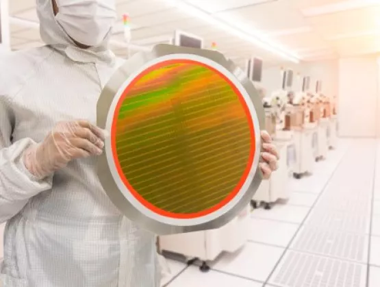
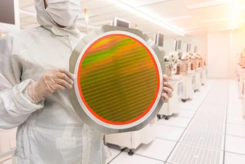
Semiconductors play an essential role in modern society by enabling ground-breaking technological advances. The manufacture of high-volume and advanced semiconductors requires the use of fluorinated chemicals known as PFAS. Representing the voice of SEMI members, I explained the important role of these substances and their “essential use” in the semiconductor manufacturing supply chain at a Chemical Watch conference for industry and European Union decision-makers on 3rd of December 2020.In order to achieve the European Green Deal’s zero pollution ambition for a toxic-free environment, the European Commission announced in its recently published Chemicals Strategy for Sustainability its intention to restrict the use of the most harmful chemicals, except in cases where they are deemed essential for society. Per- and polyfluoroalkyl substances – known as PFAS – are the first group of chemicals facing regulatory scrutiny on this basis. This begs the question: What chemicals should be characterized as essential for society and what uses will they encompass? The key and enabling role of semiconductors in modern lifeSemiconductors are essential and ubiquitous in our lives. They are integral to enabling modern society to function – driving advancements in mobile communication technologies for the smartphones and computers that help us work more efficiently and connect us with our loved ones. These benefits have never been more evident than in 2020 with billions of people finding themselves working and studying remotely and safely from home.At the same time, technologies relying on semiconductors have been vital in the effort to combat COVID-19 – in ventilators, medical imaging devices and digital healthcare solutions. In addition, semiconductors will also enable the next leap in society to Industry 4.0 and as essential building blocks in connected and electric vehicles, artificial intelligence (AI) and quantum computing.The Commissioner for Internal Market, Thierry Breton, has highlighted the strategic importance of semiconductors in achieving European digital sovereignty (for instance, in his speech at Hannover Messe Digital Days), and the EU’s New Industrial Strategy[1] also points to the importance of semiconductors and microelectronic systems. What must also be appreciated are the cost and complexity of producing these valuable technologies. Setting up a cutting-edge fabrication plant with the hundreds of pieces of semiconductor manufacturing equipment typically required can cost around €15 billion.[2] A single semiconductor manufacturing tool typically consists of millions of articles, and a typical fab may house several hundred pieces of equipment. Furthermore, according to SEMI estimates, the fabrication of semiconductor wafers requires approximately 500 highly specialized process chemicals. In many cases, these processes, equipment and facilities rely on the unique properties offered by PFAS.“SEMI has worked diligently to highlight the strategic importance of semiconductors in achieving European digital sovereignty, and we are pleased that the critical role of microelectronics has been fully recognized by the EU and Member States. Fluorinated chemicals are essential for semiconductor manufacturing. "These specific chemicals are necessary due to their unique properties, and no alternatives are currently available that can adequately provide the functional properties required in semiconductor manufacturing. The essential use concept, therefore, must enable technological innovation, must apply across the entire supply chain, and must enable EU’s critical infrastructure and strategic objectives.” What are PFAS, and why and where are they used in semiconductor manufacturing?PFAS are a broad and highly diverse group of substances with unique properties and characteristics. The Organisation for Economic Co-operation and Development (OECD) has compiled a list of approximately 4,700 substances,[3] a handful of which are used in the semiconductor manufacturing industry. These very specific chemicals are necessary due to their unique and unparalleled properties that enable them to be used in the demanding conditions of semiconductor manufacturing.Semiconductor chemicalsAt the very core of semiconductor manufacturing is the photolithography process, where microscopic geometric patterns are transferred onto a film or substrate. Photolithography specialty formulations containing fluorinated compounds are used in various steps of this process to ensure quality and reduce the probability of defects. PFAS must be used due to their low surface tension and compatibility with other chemicals. PFAS are typically no longer present in the finished product. However, there are applications where PFAS are present in the final semiconductor device, particularly in imaging semiconductors used in cameras, displays and some medical devices, amongst others. Semiconductor manufacturing equipmentPFAS are also essential to semiconductor manufacturing equipment and factory infrastructure. The exceptional combination of their heat and chemical resistance and their chemical inertness allows fluoropolymers to be used both in equipment components (tubing, gaskets, containers, filters, etc.) and lubrication (such as various oils and greases). These same properties are also needed to ensure the functioning of the surrounding infrastructure. Finally, some fluorinated gases, which are already regulated by specific legislation,[4] are used as refrigerants and to clean the facilities.These are a handful of examples of how PFAS are used in semiconductor manufacturing. Today, there is no other way to undertake these processes or to build semiconductor manufacturing equipment without PFAS. No alternatives are currently available that can adequately provide the functional properties required. Even if alternative chemicals and technologies were discovered today, due to the extremely complex qualification process throughout the value chain, it would take another 15 years to deploy them in high-volume manufacturing. Therefore, continued access to PFAS is a prerequisite for high-volume and advanced semiconductors. Lack of continued access to PFAS could lead to an inability to produce and supply the EU with semiconductor manufacturing technology.How should we think about essential uses?Regulators have started to think about what uses of PFAS are essential and in which cases their use should be allowed. In developing this concept, there are a few aspects to keep in mind.Essential use must enable, not hinder, technological innovationFirst and foremost, the essential uses concept should enable continued technological innovation instead of acting as a hindrance. Semiconductors and manufacturing technology are constantly evolving and becoming more diverse to help meet increasing societal demands. What we see as innovative today may be commonplace in the future, while future innovations may be unimaginable today. We must therefore be careful not to accidentally limit our future potential for innovation.Essential use must apply across the entire supply chainSecondly, classifying a use as essential should apply throughout the entire supply chain. We must, for example, avoid defining semiconductors as essential while classifying the semiconductor manufacturing equipment and chemicals used to produce semiconductors as not essential. In the semiconductor manufacturing supply chain, where one manufacturer can have up to 16,000 suppliers, this risk is evident.[5]Essential use must enable critical infrastructures and the EU’s strategic objectivesFinally, we should keep Europe’s societal priorities in mind. The EU needs to be able to maintain and protect its critical infrastructures. Similarly, we should not lose sight of the EU’s strategic objectives of a green and digital Europe.Semiconductors, in conjunction with their corresponding manufacturing equipment and chemicals, are essential technologies in everyday life and the backbone of the EU’s strategic value chains. Manufacturing semiconductors is a very expensive and complex process that would not be possible without the unique properties of PFAS, making them essential to achieving the EU’s strategic objectives today – whether the European Green Deal or digital autonomy – and in the future. Therefore, we must ensure that essential uses will enable the continued use of PFAS in semiconductor manufacturing.The SEMI presentation delivered at the Chemical Watch event can be accessed here.Emir Demircan is director of Public Policy and Advocacy at SEMI Europe.[1] “The EU will also support the development of key enabling technologies that are strategically important for Europe’s industrial future. These include robotics, microelectronics, high-performance computing and data cloud infrastructure, blockchain, quantum technologies, photonics [etc.]”[2] Emerging technologies in electronic components and systems (ECS) Opportunities Ahead – A study by DECISION, 2018 for the European Commission[3] Available here[4] Regulation (EU) No 517/2014, “F-Gas Regulation”[5] SIA Nathan Associates, 2016, https://www.semiconductors.org/wp-content/uploads/2018/06/SIA-Beyond-Borders-Report-FINAL-June-7.pdf
Read More
While Artificial Intelligence (AI) emerged in the 1950s, only in recent years have AI applications proliferated with the explosion of data and continuing improvements in Moore’s law that have driven rising processing speeds. Voice assistants, image analysis software, search engines, and speech and facial recognition systems were among the first applications to use AI. Today, adoption has spread to sectors such as agriculture, cybersecurity, healthcare, software development, e-government and the intelligent enterprise to generate jobs and help spur economic growth. The Edge AI Opportunity and the Microelectronics IndustryAI can be embedded in hardware devices such as advanced robots, autonomous cars, drones or Internet of Things (IoT) applications. Today, according to the EU’s digital strategy, data centres and other centralized computing facilities account for the vast majority – 80% – of AI data processing and analysis, with smart connected objects such as automobiles, home appliances and manufacturing robots that bring the compute function closer to the user representing 20%. The latter, known as Edge AI applications, are powered by edge-based machine learning chipsets, not the AI chipsets designed to run cloud-based machine learning algorithms.The EU’s white paper on AI published in February 2020 anticipates that the way data are stored and processed for AI applications will change significantly over the coming five years as edge computing applications proliferate. Most AI applications need to connect with devices that collect data and manage data flows. When the applications connect with cloud infrastructures to train large volumes of data for a machine learning model, the interface devices often require hardware support. Edge AI can minimize data transport by processing data directly from local devices to accelerate data analysis and decision-making and make data transport or accelerator hardware unnecessary, critical in reducing power consumption and enhancing data security for applications such as autonomous driving. Over the past 40 years, the ICT sector has been continuously increasing greenhouse gas (GHG) emissions despite efforts to shift to renewable energy. Cloud-based AI applications require an ICT infrastructure for high-performance computing and high-speed connectivity. According to MIT Technology Review, data centres’ AI workloads could account for a tenth of the world’s electricity usage by 2025. a mass update of cloud-based AI applications may significantly increase energy consumption, unlike with Edge AI. This is why the strategy for developing Edge AI is well-aligned with the EU’s Green Deal objectives. Europe aspires to play a leadership role in Edge AI to strengthen the sector’s competitiveness and protect the European digital sovereignty. Europe’s strong industrial competencies in embedded systems and microcontrollers will help the region promote development of European domestic AI solutions for emerging high-value IoT applications in industrial processes such as Industry 4.0, Connected and Automated driving (CSA), smart cities, climate action, healthcare, and national defence and security. With this strong strategic position in technology, Europe is well-positioned to invest to become the leader in the Edge AI global market.Preparing the Workforce for the Microelectronics IndustryTo design and manufacture leading Edge AI chipsets, European education providers and industry will need to work closely together to train the current and future workforces. Within the framework of the METIS project, a four-year project co-funded by the European Commission through the Erasmus+ programme, SEMI and imec deployed experts in the field to survey and interview focus groups. The survey identified the following key focus areas for workforce development: 1. True Capability of AI and Data Science With AI’s heavy dependence on data, the workforce of the future must be trained in areas of data science including data integrity to ensure quality, unbiased sourcing, collection and accurate analysis necessary to interpret huge volumes of data. Europe also needs to train the next generation of AI chip designers in data security and privacy – key challenges to the widespread deployment of Edge AI chips. 2. Climate Change, Sustainable Development Goals (SDGs) and Social Inclusion TrainingSince the industry must be able to develop Edge AI solutions to enable the digital transformation while limiting GHG emissions, microelectronics engineers need to be schooled in climate change and understand how their work contributes to meeting the United Nation’s Sustainable Development Goals (SDGs). Workplace diversity and social inclusion are also important target areas for education since Edge AI applications should serve various groups of people with different needs.3. EthicsChip industry workers must also be educated in ethical issues of AI related to the technology’s potential societal impact in the near future[1]. With AI applications capable of monitoring Internet searches based on users’ personal preferences and biases to deliver tailored advertising, news and other information, developers must recognize how the technology can influence thinking and behaviour of individuals and groups. This awareness can help developers strike a balance between supporting commercial interests and societal good so the microelectronics industry can ensure ethical implementation of AI. 4. Cross-disciplinary Skills Required for AIAI development requires a comprehensive, cross-disciplinary skill-set to be able to integrate the work of specialists from diverse educational, cultural and professional backgrounds critical to developing non-biased AI solutions. For example, in addition to technical expertise, microelectronics AI developers must be able to communicate clearly and work in close-knit teams with non-technical experts from business, law, medicine and the social sciences.What’s Next?The microelectronics industry has a tremendous opportunity to develop new chip-based solutions for AI architectures, and apply AI techniques to improve operational efficiencies of design and manufacturing. To seize this opportunity, the industry must work closely with education providers to groom the next generation of skilled workers. This tight collaboration is critical to designing and delivering specialised courses to college and university students as well as engineers now working in the chip sector. The stakes are high. By preparing workers to develop Edge AI chipsets, the microelectronics industry can help the world confront some of the greatest challenges it faces today.For more information, see SEMI Responds to European Commission White Paper on Artificial Intelligence.METIS is a Sector Skills Alliance project co-funded by the European Commission’s Erasmus+ Program and coordinated by SEMI. The four year project, launched in November 2019, will develop a Microelectronics Skills Strategy. Based on the strategy, the METIS project will design 43 training modules for 1,100 hours learning in four key areas of the microelectronics sector.We thank Patrick Blouet (STMicroelectronics) and Jeroen Geusens (imec) for their valuable contributions to this article.[1] Ethics of Artificial Intelligence and Robotics, Stanford Encyclopedia of PhilosophyDr. Yanying Li is senior manager of Collaborative Projects at SEMI Europe.Dr. Pushkar P. Apte is the strategic technology advisor for the Smart Data AI Initiative at SEMI
Read More
SEMI is pleased to welcome Singapore-based UTAC Holdings Ltd., formed nearly 50 years ago, as a new member. UTAC is a leading independent provider of assembly and test services for a broad range of semiconductor chips, offering a full range of semiconductor assembly and test services across analog, mixed-signal and logic, and memory. Its customers are primarily fabless companies, integrated device manufacturers and wafer foundries. The company has production facilities in Singapore, Thailand, China, Indonesia and Malaysia as well as sales offices in five regions: the United States, Japan, China, Taiwan, the rest of Asia and Europe.I recently spoke with Dr. Nathapong Suthiwongsunthorn, Vice President and General Manager of UTAC Thailand, about UTAC’s smart manufacturing advances, the company’s role in the semiconductor industry’s transformation, and the industry outlook for Thailand over the next year.Ng: How does UTAC Thailand complement your other facilities?Dr. Nathapong: As one of the world’s largest producers of quad-flat-no-leads (QFN), UTAC Thailand has significant capability in assembly and test of advanced leadframe products including power products such as Cu Clip packages as well as MEMS products. We also serve top global IDMs and have the largest share of assembly and test for the automotive market among all UTAC operations. UTAC’s other facilities have expertise in wafer-level packages and system-in-a-package and serves the communication and consumer market not only for IDMs but also for the fabless and foundry companies. The Thailand factory nicely complements the other UTAC facilities both from the standpoint of operational and marketing diversity. Ng: UTAC Holdings Ltd. announced in August this year that it has completed its sale to Wise Road Capital, a global private equity firm. Will this in any way change the operation and business strategy of UTAC Thailand?Dr. Nathapong: I don’t believe it will change the way we operate. However, the acquisition is very positive for us from a financial perspective. With the benefit of significantly reduced debt and interest expenses, we will be able to expand our business to grow with and hopefully beyond the semiconductor market. Ng: To what extent has UTAC adopted smart manufacturing?Dr. Nathapong: UTAC Thailand is leading the way in terms of automation, smart manufacturing and Industry 4.0 with our in-house automation team and unique expertise. For example, we have built our own inspection equipment that is much faster and cheaper than what is commercially available. We also working on many programs such as mobile robot, AGV, auto inspection and office automation to help drive greater production efficiency. We are replicating our manufacturing advances and fanning them out to other UTAC facilities.UTAC Thailand Ng: What are some of the challenges you face in pushing for the industrial transformation in Thailand?Dr. Nathapong: I think the key challenge is to find skilled engineers who can perform hardware- and software-related tasks critical to the industrial transformation. But frankly, we have done a good job in managing this challenge by hiring very smart people, providing them with the required in-house training, and using outside training for new recruits as necessary. We have developed partnerships with capable vendors in this regard as well.Ng: What are the key differentiating elements (e.g. talent, tax, technology, trade, EHS) in Thailand that have been instrumental in supporting the E E ecosystem?Dr. Nathapong: There are two key differentiating elements for us. Firstly, UTAC has been around for over 47 years and is very well-established in Thailand with a positive reputation as an employer. This makes hiring talented people relatively easy. Secondly, and perhaps more importantly, the nature of the Thai people and also the benefits the company provides make it relatively painless to retain key employees. I also believe that we have a significant number of engineers available in Thailand. Finally, labour costs in Thailand are still very reasonable and stable. So we are able to acquire talent at a very competitive rate compared to other countries. Ng: What is the industry outlook for E E industry in Thailand over the next year?Dr. Nathapong: Surprisingly, the current sad predicament of COVID-19 has shown no negative impact for the global semiconductor industry – people seem to be buying more electronics with the lockdown. Our outlook for the Thailand’s E E industry is similarly very positive. Most semiconductor companies including UTAC see significant growth this year and I hope it will continue.Ng: With the recent semiconductor geopolitical and trade tensions, are more customers moving their business to Thailand?Dr. Nathapong: I believe so. We do see some of our key customers move manufacturing out of China and into Thailand. The relocations help them offset or avoid any potential fallout from current geopolitical tensions.Ng: In what areas do you think SEMI Southeast Asia can play a role to help our members companies in Thailand like UTAC?Dr. Nathapong: The semiconductor industry has been in Thailand for a long time. In fact, UTAC Thailand is 47 years old this year! However, I feel that Thailand never really worked with a strong establishment organization like SEMI that can connect various companies together to help drive innovation. I think SEMI Southeast Asia can truly help Thailand to move up to the next level of providing semiconductor solutions globally. We welcome SEMI Southeast Asia’s help in this regard.About Dr. Nathapong SuthiwongsunthornDr. Nathapong Suthiwongsunthorn joined UTAC in 2009 and is currently General Manager of UTAC Thailand, UTAC’s largest operation site. Before taking over the management of Thailand operations, he was Vice President of Research and Development, running UTAC’s global R D group. Dr. Nathapong has more than 20 years of experience in the semiconductor industry. He holds more than 40 international patents and publications in wafer-level and advanced packaging.Prior to joining UTAC, Dr. Nathapong held several key leadership positions in research and development at Schott, STATS ChipPAC and Infineon. Dr. Nathapong has a Ph.D. in Electronics Engineering from Oxford Brookes University, England.Bee Bee Ng is president of SEMI Southeast Asia.
Read More
METIS, a Sector Skills Alliance project co-funded by the European Commission’s Erasmus+ Program and coordinated by SEMI, recently launched an online questionnaire aimed at gauging the skills and expertise the industry needs to drive continued growth over the next five years. The survey, which will stay online until 15 October 2020, is a part of the METIS project’s efforts to involve a broad range of stakeholders in the microelectronics industry to assess workforce, future technology and economic trends influencing talent development and the skills needed most today and in the next five years. The survey aims to highlight the skill mismatches in specific job profiles that are of increasing importance to the microelectronics industry. It elaborates on the upskilling and reskilling needs for design engineers. Given that semiconductor design is becoming increasingly crucial for Europe’s competitiveness and technological sovereignty, the new skills required from design engineers are a priority area for the METIS project. Other examples are the manufacturing and maintenance technicians, two job profiles that are currently experiencing significant shifts in their skillsets, as COVID-19 has thoroughly transformed their way of work.While the microelectronics industry has been very aware of the importance of the high level of investment in R D, it is equally crucial to ensure that the workforce of the industry is equipped with knowledge and skills for the rapid technological developments. Maintaining high levels of investment in workforce including attracting talent, updating their knowledge and skills with the latest technological development, and supporting them to lead innovations, is essential for this industry. There is a growing demand for specific requirements for this sector to support innovation in many other sectors such as automotive, energy, healthcare, and government, to foster benefits from emerging digital technologies such as Cloud Services, Internet of Things (IoT), Artificial Intelligence (AI), Digital Reality, and Blockchain.In addition to the online questionnaire, the METIS project consortium is interviewing top experts from leading microelectronics companies, education representatives from universities and training academies, and experts from government agencies and industry associations. The interview outcomes provide inputs on what kind of employee profiles are the most difficult to find, what skills this sector is looking for in a candidate, and what kind of training and policy frameworks are needed to improve employers’ skills. Those inputs are essential to develop the skill strategy and form recommendations on training modules.Furthermore, the METIS project consortium is organizing 10 focus groups. Each of the focus groups is dedicated to a key topic, such as SC design, SC materials, semiconductor manufacturing equipment, etc. For example, one of the METIS focus groups is dedicated to Edge AI, a top priority for the microelectronics industry. Strengthening the AI talent pipeline is essential to harness the potential of Edge AI in Europe and to facilitate the shift from the Cloud to the Edge when possible in order to meet specific demands (e.g. for autonomous driving), reduce energy consumption for data communications, and to increase efficiency. The EU’s White Paper “Artificial Intelligence - A European approach to excellence and trust”[1] , published this February, also emphasizes the importance of upskilling and reskilling to position Europe among the global leaders in AI. Hence, the focus group will work towards pinpointing the skills necessary for the semiconductor workforce to capture the potential of the trend.The results of the survey, interviews and focus groups will be used to form the Microelectronics Skills Strategy. Based on this strategy, the METIS project will design 43 training modules for 1,100 hours learning in four key areas of the microelectronics sector:Component designSystem designBasic of manufacturingKey competencies and innovative thinkingThe METIS project is planning to recruit 2,000 learners in companies and education and training institutes to participate in the trainings and validate the impact. The METIS project will also work with companies, education and training providers to ensure continuity of the initiative and foster cooperation.During the METIS project course (2019 – 2023), the Skills Strategy will be updated yearly to reflect the latest technology and market trends. To enable the Skills Strategy to continue serving the industry, METIS is working on forming a permanent instrument, named Observatory and Skills Council, to continue developing the skills strategy, update the training and facilitate cooperation between industry and education and training providers.Laith Altimime, president of SEMI Europe, and 50 members of the Microelectronics Training, Industry and Skills (METIS) consortium The METIS consortium invites companies and associations involved in microelectronics training and education provision, human resources and career services professionals, technology strategists and policy makers to complete the online questionnaire. Stakeholders are also welcome to subscribe to the METIS newsletter for the latest on METIS programs. For more details, please contact Yanying Li at [email protected].[1] EU’s White Paper on Artificial Intelligence available at: https://ec.europa.eu/info/sites/info/files/commission-white-paper-artificial-intelligence-feb2020_en.pdfDr. Yanying Li is senior manager of Collaborative Projects at SEMI Europe.
Read More
Many companies are applying Fourth Industrial Revolution initiatives in manufacturing, though only a few have managed to successfully integrate the smart manufacturing technologies at a scale that allows them to realise significant economic and financial benefits.Known as lighthouse companies, these organisations have taken their smart manufacturing journeys from pilot to integration at scale, serving as beacons to others in overcoming challenges in their production systems through the adoption of leading-edge technologies such as artificial intelligence, additive manufacturing and advanced analytics.At the recent SEMI Southeast Asia webinar Journey to Recovery of the E E Industry, Dato' Azman Mahmud, Chief Executive Officer of Malaysian Investment Development Authority (MIDA), spoke about building Malaysia’s very own Lighthouse Project comprising multinational corporations that will act as anchors to help guide local players into this new venture.During the webinar, Dato' Azman elaborated about Malaysia’s competitive edge – its diversified economic structure and government support. He said the key to sustaining this competitive edge, however, is that the Malaysian economy must be digitally empowered. The Lighthouse Project is one programme that will help achieve this objective. We are inspired and encouraged by this initiative. As firm believers in connecting and collaborating, SEMI Southeast Asia supports programmes that advance the entire microelectronics ecosystem. We look forward to seeing MIDA drive this project, and we encourage Malaysian E E companies to tap MIDA’s expertise in this field. Ultimately, we are confident that through this initiative and the adoption of Industry 4.0 technologies, Malaysia will be repositioned as a top global manufacturing nation. Bee Bee Ng is president of SEMI Southeast Asia.
Read More
As artificial intelligence’s (AI) sprawling influence reshapes industries from logistics and healthcare to automotive and manufacturing, Taiwan is poised to leverage its cutting-edge capabilities and rich history in semiconductor manufacturing to stake out a leadership position in AI. Taiwan’s semiconductor manufacturing industry accounts for a major share of the region’s GDP and, with its manufacturing prowess, the region is fertile ground for using AI to optimize and even revolutionize chip manufacturing. In an AI and Semiconductor Smart Manufacturing Forum recently hosted by SEMI Taiwan, experts from Micronix, Advantech, Nvidia and the Ministry of Science and Technology of Taiwan (MOST) shared their insights on how deep learning, data analytics and edge computing will shape the future of semiconductor manufacturing. Here are four key takeaways.1. Monitor, Forecast, and PreventToday, tier 1 foundries use AI tools to combine equipment know-how and manufacturing statistics in managing massive Fault Detection (FD) data, much in the way that a car’s tire-pressure monitoring system helps maintain safe inflation levels and prevent accidents. For example, AI enables the real-time collection and monitoring of massive amounts of processing data, then alerts system administrators of any hardware failures or other manufacturing abnormalities.AI also makes it possible to adopt Run-to-Run (R2R) control to automate manufacturing process adjustments and corrections by providing feedback that can drive higher processing efficiency. In addition, virtual metrology replaces manual sampling inspection for comprehensive quality control, enabling foundries to improve yields, reduce costs, and strengthen their competitive advantage.2. Beyond Automation: Edge Computing The evolution of IoT is giving rise to a paradigm shift in the industry as the recognition grows that smart factories must go beyond automation to focus also on intelligence. All information – from equipment status and manufacturing process statistics to on-site environmental data – needs to be collected through sensors. In highly time-critical scenarios, returning all sensor data to the cloud for processing is time-consuming and impracticable. This is where edge computing’s real-time features and lower cost than cloud computing come into play.How does edge computing work in a smart factory? First, a rich trove of data from various devices is collected and integrated via Manufacturing Execution Systems (MES). Software analysis then produces a real-time factory production status before production data is visualized through a combination of system platforms and human-machine interfaces. In the end, the data is analyzed realtime in the cloud so failures can be predicted and prevented to help increase capacity and reduce costs. The approach is even capable of Bill of Materials (BOM) predictions, allowing better collaboration between upstream and downstream suppliers.3. Deep Learning Accelerates AI Deep learning enables autonomous driving, intelligent voice assistance and many other AI breakthroughs. The heart of deep learning is its ability to automatically process and learn data in various formats such as images, video and text with no human domain knowledge. This increases predictive accuracy and efficiency in processing massive amounts of data. Deep learning also enhances the efficiency of human-machine collaboration.4. Taiwan’s Competitive Niche: Industry 3.5Industry 4.0 is not just about improving production management. It also focuses on integrating supply chains, even among competitive companies. For Industry 4.0 to thrive, rival companies must grow together. The first and third industrial revolutions centered on disruptive technologies like steam engines, transistors and digital, while the second and fourth revolutions homed in on competition among various business models, platforms and industry ecosystems.While Taiwan’s strengths include innovation, short time-to-market, low manufacturing costs, and high supply chain management efficiency, the region still lags advanced countries in basic industry and research capabilities. Squeezed by Chinese supply chains and high-end manufacturers in advanced countries, Taiwan should start by carving out an Industry 3.5 niche for the island’s manufacturers. SEMI will continue to facilitate cross-industry connection, collaboration and innovation to help manufacturers seeking higher production efficiency and lower costs incorporate AI as a core competitive advantage. At SEMICON Taiwan 2018, SEMI will unveil its Smart Manufacturing Journey, an exhibition that gathers leading AI companies such as ABB, Advantech, Nvidia, Sony and UPS to demonstrate a comprehensive roadmap for smart manufacturing technologies and applications. For more information, please visit the SEMICON Taiwan website.Emmy Yi is a marketing specialist at SEMI Taiwan.
Read More