downloadGroupGroupnoun_press release_995423_000000 copyGroupnoun_Feed_96767_000000Group 19noun_pictures_1817522_000000Member company iconResource item iconStore item iconGroup 19Group 19noun_Photo_2085192_000000 Copynoun_presentation_2096081_000000Group 19Group Copy 7noun_webinar_692730_000000Path
Skip to main content
Default Banner Image

electric vehicles

In my role as lead for the Smart Mobility initiative at SEMI, I recently spoke with Automotive Logistics Magazine about the growing importance of the semiconductor supply chain’s connection with the automotive industry and the semiconductor shortage hampering global automotive production. Following are excerpts from the interview. Automotive Logistics: Why is there a bottleneck in the global supply of semiconductors at the moment and how long is it likely to last? Weiss: The current automotive chip shortage resulted from the sharp, Covid-19-induced decrease in demand for automotive semiconductors in the second quarter of last year when vehicle production came to a near standstill. The automotive market picked up significantly in the fourth quarter and this caused the supply chain constraints we are seeing today. At the same time as the automotive standstill, the pandemic spurred an increase in demand for home computing and networking equipment, and semiconductor manufacturing plants (fabs) had to pivot to these other markets in order to maximize fab utilization and successfully navigate economic headwinds. Every minute a semiconductor fab is idle or has lines down adds up quickly to missed revenue, so their capacity is booked weeks and even months in advance. With this background, I don’t believe this is a structural shortage and expect a gradual recovery over the next two quarters, barring any major shifts in geopolitics or macroeconomics. Automotive Logistics: What needs to be done to remedy the current shortfall for the automotive industry? Weiss: The automotive industry needs to continue to strengthen its connections to the semiconductor manufacturing supply chain. In past years, auto manufacturers used to rely mainly on their tier one suppliers to interface with the semiconductor supply chain. This has changed significantly. Not only are more chips being used in vehicles (roughly 10% of all devices produced globally end up in cars), but the strategic importance of the chips as enablers for ADAS [advanced driver-assistance systems], electrification, safety, connectivity and other consumer-driven features has increased considerably. With this dynamic in play, carmakers have recognized the value of interacting and collaborating more closely with the semiconductor supply chain. This provides vehicle OEMs with access to innovation, the ability to influence technology direction and pace, along with greater visibility into global supply chain developments. The SEMI Smart Mobility initiative is evidence of this transition, with the likes of Audi, BMW, Ford, Uber, Volkswagen and other vehicle OEMs, along with tier one suppliers such as Continental and Bosch, now actively involved in our automotive electronics and mobility activities to do exactly that – influence, partner, accelerate and guide the global electronics design and manufacturing supply chain that SEMI represents. Automotive Logistics: What percentage of semiconductors manufactured for use by US-based companies are for automotive applications and how has this grown in recent years? Weiss: A little over 10% of semiconductors produced worldwide are sold into the automotive segment, but this number is expected to grow at an accelerated pace in the next few years as electrification, connectivity and autonomous driving become more prevalent. Automotive Logistics: How is SEMI working to help the automotive industry get a clearer view of sub-component supply and better manage supply chain risk? Weiss: The SEMI Smart Mobility initiative is designed to engage automotive OEMs, tier ones, semiconductor device makers, design houses, and equipment and materials companies to drive alignment across the supply chain and address shared challenges collectively. To facilitate this engagement, we created the Global Automotive Advisory Council (GAAC), which has active chapters in Europe, US, China, Japan and Taiwan. The GAAC provides an open platform for creating solutions, fostering collaboration and partnering with other industry bodies to accelerate and harmonize industry efforts that benefit the entire ecosystem. Volkswagen and Audi are already SEMI members – both are founding members of the GAAC Europe chapter – and have become vocal champions and critical contributors to our efforts. When all stakeholders work together, I have no doubt that the future of automotive and mobility will continue to be bright. Interested in learning more about this topic? Read the full interview in Automotive Logistics Magazine, A Fab Future for the Automotive Sector. Please contact me at [email protected] for more information about SEMI’s Smart Mobility Initiative, the Global Automotive Advisory Council, and how SEMI can help your organization navigate electronics in the automotive industry to drive innovation in the mobility space. Bettina Weiss is Chief of Staff and Global Smart Mobility Lead at SEMI.
Read More
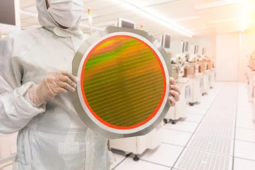
Semiconductors play an essential role in modern society by enabling ground-breaking technological advances. The manufacture of high-volume and advanced semiconductors requires the use of fluorinated chemicals known as PFAS. Representing the voice of SEMI members, I explained the important role of these substances and their “essential use” in the semiconductor manufacturing supply chain at a Chemical Watch conference for industry and European Union decision-makers on 3rd of December 2020.In order to achieve the European Green Deal’s zero pollution ambition for a toxic-free environment, the European Commission announced in its recently published Chemicals Strategy for Sustainability its intention to restrict the use of the most harmful chemicals, except in cases where they are deemed essential for society. Per- and polyfluoroalkyl substances – known as PFAS – are the first group of chemicals facing regulatory scrutiny on this basis. This begs the question: What chemicals should be characterized as essential for society and what uses will they encompass? The key and enabling role of semiconductors in modern lifeSemiconductors are essential and ubiquitous in our lives. They are integral to enabling modern society to function – driving advancements in mobile communication technologies for the smartphones and computers that help us work more efficiently and connect us with our loved ones. These benefits have never been more evident than in 2020 with billions of people finding themselves working and studying remotely and safely from home.At the same time, technologies relying on semiconductors have been vital in the effort to combat COVID-19 – in ventilators, medical imaging devices and digital healthcare solutions. In addition, semiconductors will also enable the next leap in society to Industry 4.0 and as essential building blocks in connected and electric vehicles, artificial intelligence (AI) and quantum computing.The Commissioner for Internal Market, Thierry Breton, has highlighted the strategic importance of semiconductors in achieving European digital sovereignty (for instance, in his speech at Hannover Messe Digital Days), and the EU’s New Industrial Strategy[1] also points to the importance of semiconductors and microelectronic systems. What must also be appreciated are the cost and complexity of producing these valuable technologies. Setting up a cutting-edge fabrication plant with the hundreds of pieces of semiconductor manufacturing equipment typically required can cost around €15 billion.[2] A single semiconductor manufacturing tool typically consists of millions of articles, and a typical fab may house several hundred pieces of equipment. Furthermore, according to SEMI estimates, the fabrication of semiconductor wafers requires approximately 500 highly specialized process chemicals. In many cases, these processes, equipment and facilities rely on the unique properties offered by PFAS.“SEMI has worked diligently to highlight the strategic importance of semiconductors in achieving European digital sovereignty, and we are pleased that the critical role of microelectronics has been fully recognized by the EU and Member States. Fluorinated chemicals are essential for semiconductor manufacturing. "These specific chemicals are necessary due to their unique properties, and no alternatives are currently available that can adequately provide the functional properties required in semiconductor manufacturing. The essential use concept, therefore, must enable technological innovation, must apply across the entire supply chain, and must enable EU’s critical infrastructure and strategic objectives.” What are PFAS, and why and where are they used in semiconductor manufacturing?PFAS are a broad and highly diverse group of substances with unique properties and characteristics. The Organisation for Economic Co-operation and Development (OECD) has compiled a list of approximately 4,700 substances,[3] a handful of which are used in the semiconductor manufacturing industry. These very specific chemicals are necessary due to their unique and unparalleled properties that enable them to be used in the demanding conditions of semiconductor manufacturing.Semiconductor chemicalsAt the very core of semiconductor manufacturing is the photolithography process, where microscopic geometric patterns are transferred onto a film or substrate. Photolithography specialty formulations containing fluorinated compounds are used in various steps of this process to ensure quality and reduce the probability of defects. PFAS must be used due to their low surface tension and compatibility with other chemicals. PFAS are typically no longer present in the finished product. However, there are applications where PFAS are present in the final semiconductor device, particularly in imaging semiconductors used in cameras, displays and some medical devices, amongst others. Semiconductor manufacturing equipmentPFAS are also essential to semiconductor manufacturing equipment and factory infrastructure. The exceptional combination of their heat and chemical resistance and their chemical inertness allows fluoropolymers to be used both in equipment components (tubing, gaskets, containers, filters, etc.) and lubrication (such as various oils and greases). These same properties are also needed to ensure the functioning of the surrounding infrastructure. Finally, some fluorinated gases, which are already regulated by specific legislation,[4] are used as refrigerants and to clean the facilities.These are a handful of examples of how PFAS are used in semiconductor manufacturing. Today, there is no other way to undertake these processes or to build semiconductor manufacturing equipment without PFAS. No alternatives are currently available that can adequately provide the functional properties required. Even if alternative chemicals and technologies were discovered today, due to the extremely complex qualification process throughout the value chain, it would take another 15 years to deploy them in high-volume manufacturing. Therefore, continued access to PFAS is a prerequisite for high-volume and advanced semiconductors. Lack of continued access to PFAS could lead to an inability to produce and supply the EU with semiconductor manufacturing technology.How should we think about essential uses?Regulators have started to think about what uses of PFAS are essential and in which cases their use should be allowed. In developing this concept, there are a few aspects to keep in mind.Essential use must enable, not hinder, technological innovationFirst and foremost, the essential uses concept should enable continued technological innovation instead of acting as a hindrance. Semiconductors and manufacturing technology are constantly evolving and becoming more diverse to help meet increasing societal demands. What we see as innovative today may be commonplace in the future, while future innovations may be unimaginable today. We must therefore be careful not to accidentally limit our future potential for innovation.Essential use must apply across the entire supply chainSecondly, classifying a use as essential should apply throughout the entire supply chain. We must, for example, avoid defining semiconductors as essential while classifying the semiconductor manufacturing equipment and chemicals used to produce semiconductors as not essential. In the semiconductor manufacturing supply chain, where one manufacturer can have up to 16,000 suppliers, this risk is evident.[5]Essential use must enable critical infrastructures and the EU’s strategic objectivesFinally, we should keep Europe’s societal priorities in mind. The EU needs to be able to maintain and protect its critical infrastructures. Similarly, we should not lose sight of the EU’s strategic objectives of a green and digital Europe.Semiconductors, in conjunction with their corresponding manufacturing equipment and chemicals, are essential technologies in everyday life and the backbone of the EU’s strategic value chains. Manufacturing semiconductors is a very expensive and complex process that would not be possible without the unique properties of PFAS, making them essential to achieving the EU’s strategic objectives today – whether the European Green Deal or digital autonomy – and in the future. Therefore, we must ensure that essential uses will enable the continued use of PFAS in semiconductor manufacturing.The SEMI presentation delivered at the Chemical Watch event can be accessed here.Emir Demircan is director of Public Policy and Advocacy at SEMI Europe.[1] “The EU will also support the development of key enabling technologies that are strategically important for Europe’s industrial future. These include robotics, microelectronics, high-performance computing and data cloud infrastructure, blockchain, quantum technologies, photonics [etc.]”[2] Emerging technologies in electronic components and systems (ECS) Opportunities Ahead – A study by DECISION, 2018 for the European Commission[3] Available here[4] Regulation (EU) No 517/2014, “F-Gas Regulation”[5] SIA Nathan Associates, 2016, https://www.semiconductors.org/wp-content/uploads/2018/06/SIA-Beyond-Borders-Report-FINAL-June-7.pdf
Read More
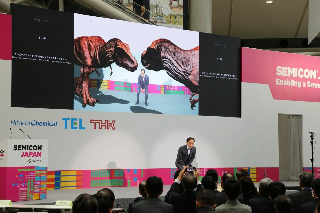
Augmented reality (AR) tyrannosauruses towered on-screen as I interacted with the creatures in a mix of prehistoric and cutting edge. Or, rather, my AR double was doing the playacting. Minutes later, virtual doppelgangers of a small lineup of chip industry executives cut the ceremonial ribbon. Seemingly sweeping away the winter chill, the opening of SEMICON Japan 2019 dazzled with smart technology and the promise of lives, cities and workplaces transformed, with uber-intelligent applications in full display at Tokyo Big Sight. But what resources does the industry need to harness to drive the next era of innovation? The semiconductor industry’s unwavering passion and young talent are key, said Hiroshi Imano, Chairperson of the SEMICON Japan Initiatives Committee, in his opening keynote. And hardly any region of the world is in a better position to help realize that future than Japan, Imano said. The region supplies one third of the equipment and more than half of all materials to the global semiconductor manufacturing industry.Talent was also top of mind for SEMICON Japan 2019 keynote speaker Makiko Eda, Japan's Chief Representative Officer at the World Economic Forum (WEF). Serving as a platform for public-private partnerships, the organization's mandate is to tackle global issues such as climate change and geopolitical strife in making world more resilient to risk and, by extension, more sustainable.Spanning ecology, economy, technology, society, geopolitics and industry, that mission includes reskilling and upskilling a billion people over the next decade, a high priority for WEF, which hosts a conference every January in Davos, Switzerland. The theme of this month's conference – Stakeholders for a Cohesive and Sustainable World – reflects the vital importance of building the international partnerships and global consensus necessary to achieving WEF's goals.One key to that sustainability will be technology and Arm, a global chip design company, will play a key role, with the company’s chips touching over 70 percent of the world’s population, Arm president Yuzuru Utsumi said in his keynote. Today, Arm is driving toward an ambitious goal: Ship 100 billion chips from 2017 to 2021 – the same number produced over the previous quarter century – by powering advances in mobile computing, server and networking infrastructures, and automotive applications.Arm’s innovation ecosystem of more than 1,000 partners will deliver these chips as they continue to work together to develop differentiated technology. Arm plans to increase investments not only in its primary processor business to accelerate market share gains but in the company’s new IoT business to create new revenue streams. The goal: Deliver long-term sustainable growth, Utsumi said. SEMICON Japan 2019 showcases SMART manufacturing and transportation Billed as a showcase of smart technologies, SEMICON Japan 2019 delivered with an array of eye-grabbing exhibitions in the popular SMART Applications Zone. In the SMART Transportation area, the automatic operation pavilion featured a car equipped with open-source software for autonomous driving. The exhibitor, Tier IV, aims to help lead the early commercialization of self-driving vehicles through the adoption of its software, Autoware, which makes it easier to develop self-driving vehicle prototypes using low-power platforms.Sony Semiconductor Solutions demonstrated a vision sensing processor designed to guide autonomous drones. Using two cameras, the processor measured the changing distance between visitors moving about the exhibit and stationary objects in real time, indicating proximity in hues of red (nearby) and blue (at a distance). Many visitors were wowed, describing the multichromatic display as futuristic.Others rode a simple wooden swing hanging by two ropes, but from dizzying heights thanks to Solidray’s Duo-Sight, a virtual reality (VR) system that projects 3D images stretching from wall to floor for immersive experiences. One visitor thrilled at how riding the swing, suspended only a few feet from the floor, felt like soaring on a flying trapeze. Target applications for the technology include virtual rides at amusement parks and presenting interior design options to homeowners.In the SMART Manufacturing area, one highlight was the demonstration by the National Institute of Advanced Industrial Science and Technology (AIST) of a remote-controlled Minimal Fab System designed for low-volume, high-mix chip production with little staffing. Designed to increase production efficiency, the system allows a circuit designer to manufacture a semiconductor by singlehandedly operating equipment up and down the production line. Controlling nearly 50 pieces of equipment, the Minimal Fab System on display manufactured chips that were verified for functional operation and exhibited afterwards.On the SMART Applications stage, exhibitors DENSO and Toyota Motor Corporation announced a new joint venture to conduct research and advanced development of the next-generation in-vehicle semiconductors critical to electric and autonomous vehicle innovation. The venture, operating as MIRISE Technologies, will combine Toyota’s mobility expertise with DENSO’s in-vehicle component prowess. The goal is to build a rapid, competitive development system by 2030, said Yoshifumi Kato, executive director of the DENSO Research and Development Center, and president and representative director of the venture. On track to begin work this year, MIRISE will span three fields of technology development: power electronics, sensing and SoC (System-on-a-Chip). The name MIRISE combines word the Japanese word "mirai" (future) with "rise."Business Continuity PlanningNatural disasters and other emergencies are an ongoing threat to uninterrupted business operations across the semiconductor manufacturing supply chain and particularly in earthquake-prone Japan. To better prepare for business disruptions and restore normal operations as soon as possible after disaster strikes, more companies are teaming on Business Continuity Planning (BCP).THK's Seismic Isolation Experience Car demonstrated one technology designed to help – a seismic isolation device. The car shakes like an earthquake to give people inside a taste of how a building heaves and sways during a quake with and without the device deployed. Visitors were struck by how much the isolator dampens tremors to prevent or minimize damage. In the BCP seminar, representatives from Sony Semiconductor Manufacturing, THK, DISCO and Team Engineering Consulting shared lessons learned from actual disasters and discussed the critical importance of daily disaster drills. Yukihide Keigo, Executive Engineer in charge of Products and Development at Sony Semiconductor Manufacturing, recounted how the company’s Kumamoto Prefecture plant struggled for 96 days to restore full operations after the facility sustained heavy damage in the 2016 earthquake. Keigo said the plant lacked the structural reinforcements necessary to withstand the impact and fell prey to poor planning and accountability. The Kumamoto plant has since implemented measures – structural and procedural improvements – that more accurately account for seismic risks to ensure full recovery within 56 days. The plant’s new procedures include emergency drills for staff including night-shift workers.Innovation abounds at six SuperTHEATER forumsSEMICON Japan 2019 was held in the West and South Halls of Tokyo Big Sight as organizers of the Tokyo Olympics occupied the East Hall, the exhibition's usual home at the venue, to prepare for the 2020 games. For the first time, the main stage, SuperTHEATER, was set up in the cavernous arena near the main entrance. The SuperTHEATER featured six forums over three days. Semiconductor Executive Forum – View by Top Two in the Era of Digitalization with thought leaders from IHS Markit and Sony Semiconductor Solutions SMART Connectivity Forum – Infinite World Brought by 5G Innovation with experts from Softbank and Nokia Solutions Networks SMART Transportation Forum I – Front-line of Automated Driving featuring speakers from Intel and DENSO SMART Transportation Forum II – Revolution of Sky Transportation, supported by the U.S. Commercial Service in Japan, with presenters from Ministry of Economy, Trade and Industry (METI), Subaru and Bell Helicopter Manufacturing Innovation Summit – Issues and Innovation: What will Drive Growth to 2030 featuring thought leaders from VLSI Research, Applied Materials, KLA, Nikon and Tokyo Electron Mirai Vision Forum – Future Relation of Technology and Body 2.0 with speakers from Leave a Nest, Ory Lab and Autonomous Control Systems Laboratory The Mirai Vision Forum highlighted advanced technologies that could lead to societal improvements. One presenter, Kentaro Yoshifuji, CEO at Ory Lab, recalled how, as a child, he once stayed home from school while recovering from an illness. His imagination in full flight, the youngster imagined having a clone that could attend school and be with his classmates. The experience eventually inspired him to develop OriHime, a robot that gives socially isolated people a way to communicate with friends or colleagues remotely. Originally developed for physically impaired people, OriHime today is used to help the able-bodied. The robot is situated with the companion and the user operates OriHime remotely. A camera and monitor in OriHime’s face provide the visual and audio connection and the user controls the device with a smartphone or tablet or, for those who are paralyzed, through eye movement. One potential application: With OriHime stationed at a business office, working mothers could use OriHime to telecommute to better balance their careers with their parenting responsibilities at home. The robot would be a mother’s go-between, enabling her to communicate directly with colleagues.The next generation of innovators also took the stage as five teams presented innovative business ideas in friendly competition. The top prize in The TECH CAMP Hackathon went to the group that hatched an ingenious plan to develop a jacket that trains users to move their bodies in preprogrammed ways. For example, legendary Japanese professional baseball player Shigeo Nagashima could wear the gear while batting to program the device, then give the jacket to someone who’s never swung a baseball bat. The jacket would help the user replicate Nagashima’s swing. Now comes the real work of any innovator – executing on the vision.And then came two soccer-playing artificial intelligence (AI) robots that squared off and ... Scored! The demonstration by the Toyota National College of Technology started as a research project by Toyota National College students in 2002. The young innovators designed and developed all the robotic hardware and software from scratch. Looking ahead to SEMICON Japan 2020!SEMICON Japan 2019 not only gathered leading Japanese semiconductor materials and manufacturing equipment providers to demonstrate their latest innovations. The premiere regional event also provided insights on key trends critical to the entire electronics manufacturing supply chain. This year’s event drew more than 51,000 visitors and 695 exhibitors from 15 regions filling more than 1,700 booths.SEMICON Japan 2020 returns to East Hall at Tokyo Big Sight in December 2020. I look forward to seeing you there!Jim Hamajima is president of SEMI Japan.
Read More