Showing 985 - 996 of 8993
SEMI Press Release
SEMI University Launches In-Person Courses to Help Semiconductor Industry Workforce Build Skills, Advance in Careers
MILPITAS, Calif. — April 9, 2024 — Aiming to help the global semiconductor workforce expand its skills to address the talent gap, SEMI today announced the expansion of the SEMI University™ learning...
Blog
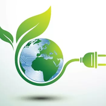
Semiconductor Sustainability: Edwards Vacuum Strategic Insights
Sustainability and climate change are hot topics among the young, who are given to environmentally-mindedness, and have become a focal point of discussions amongst global government leaders and...
SEMI Press Release
Phoenix to Host SEMICON West 2025 for the First Time, Showcasing Arizona’s Critical Role as a Semiconductor Manufacturing Hub
Event registration now open, with expanded programming and support from key Arizona partnersMilpitas, CA – June 16, 2025 — SEMI, the industry association serving the global semiconductor and...
Blog
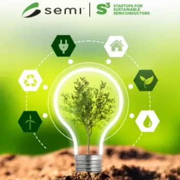
Finalists for SEMI Startups for Sustainable Semiconductors to Present Live Pitches at SEMICON West 2025
The SEMI Startups for Sustainable Semiconductors (S3) program announced 15 startups chosen as finalists for pitching to the industry at SEMICON West 2025 in Phoenix, Arizona. The finalists were...
SEMI Press Release
SEMI ISS Europe 2026 Opens Tomorrow as Leaders Convene to Navigate Geopolitics and Reinforce European Semiconductor Industry's Competitiveness
SOPOT, Poland ─ March 10, 2026 –The SEMI Industry Strategy Symposium Europe (ISS Europe) 2026 is set to open tomorrow in Sopot, Poland, convening top executives, industry...
SEMI Press Release
SEMI Americas and Semiconductor Digest Announce 2019 “Best of West” Award Finalists: CyberOptics, Advantest and Edwards
MILPITAS, Calif. – July 1, 2019 – SEMI and Semiconductor Digest today announced finalists for the Best of West award to be presented at SEMICON West 2019, July 9-11 at the Moscone Center in San...
Page
FEMC#21 Navigating the Legal Landscape: AI Litigation Risks in Semiconductor and Medtech Recording
In this webinar, Jenny Colgate and Mark Rawls, experienced “high technology” litigators, explore the emerging legal challenges posed by artificial intelligence in both the semiconductor and medtech...
Member Company
InnoLas Semiconductor GmbH
Wafer Laser Marking and Sorting Systems Standard Equipment for 2"-450mm wafer diameter available Material: Silicon, GaAs, GaN, Germanium, SiC, Quartz, LiN and 3/5 materials available Standard...
SEMI Press Release
SEMICON Japan 2022 Opens Tomorrow to Showcase Cutting-Edge Technologies Powering Semiconductor Industry Growth
Opening keynote panel to feature Rapidus representatives discussing strategies for strengthening Japan’s semiconductor industry.
TOKYO ─ December 13, 2022 ─ SEMICON Japan, the largest and most...
Member Company
Frontier Semiconductor
FSM provides wafer metrology systems including FSM 413AA for thickness, TTV, TSV, roughness, step height, and bump height. FSM 128, 500, and 900 Series measure film stress from room temperature up to...