March 8, 2023 - March 9, 2023
Interaction of Substrate and PCB to Microelectronics Packaging Assembly and Reliability
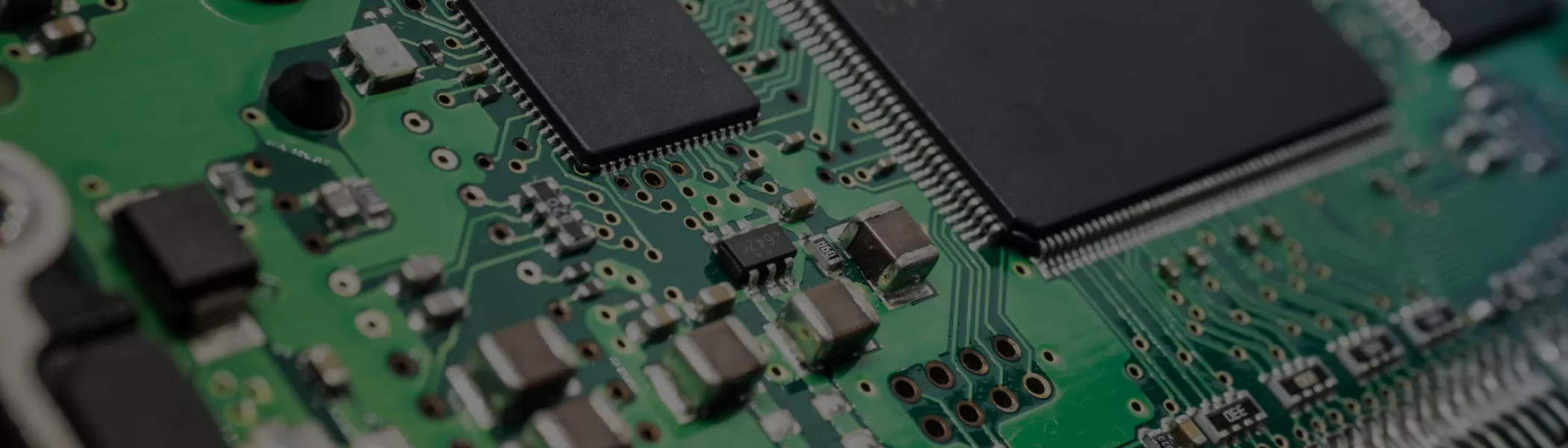
Substrate and PCB technologies are the building blocks for Microelectronics Packaging and surface mount packages.
Course Fee:
Member Rate: SGD 750
Non-member Rate: SGD 935
Register before 6 March 2023 to enjoy Early Bird rate of up to 15% off the rates above.
This workshop is HRDC Claimable, subjecting to terms and conditions.
Certificate of completion will be awarded at the end of the workshop.
Location
Malaysian International Trade & Exhibition Centre (MITEC)
No. 8 Jalan Dutamas 2
50480 Kuala Lumpur
Kuala Lumpur
Malaysia
This course will cover:
-
Substrate and PCB fabrication processes and its key processes and materials such as ABF, BT, FR5, etc.
-
Build-up micro-via technologies with use of lasers, plasma, photo materials etc.
-
Registration and tolerances of substrate design in relation to substrate and PCB fabrication processes which includes via to pattern, pattern to resist etc, which can affect microelectronics assembly processes.
-
Materials, design and surface finishes (Cu, NiAu, ENIG , NiPdAu etc) with respect to assembly processes and parameters.
-
Substrate defects and package reliability including failure of fatigue, kirkendall voids and intermetallics.
Why should I attend?
- Provides necessary technical knowledge for industry professionals
- Enhance knowledge in manufacturing and R&D know-how in IC packaging
- Case studies discussion
- Networking Opportunity with industry peers
Who should attend?
- Directors, managers, process engineers, R&D engineers working in the areas of microelectronics
- Useful for sale or application engineers who supply packaging materials and tools to the industry

Agenda
Note: Program is subject to changes.
Opening Address by Invest Selangor
Substrate & PCB Materials and Fabrication Flow
- Introduction
- Core Materials – FR4, BT, ABF etc.
- Key Processes
- Mechanical, laser drilling
- Patterning exposure, develop, etch, strip
- Electroless and electrolytic plating
- Lamination and buildup
- 2 Layer fabrication flow
Lunch
Design and Tolerances Affecting Packaging
- Mechanical registration and tolerances
- Cu patterning registration and tolerances
- Solder registration and tolerances
- Substrate challenges and constraints
- Plating finishes
- Problem solving exercises on Assembly Challenges
Q&A Discussion
End of Day 1
Assembly Challenges and Defects
- Assembly differences in PCB and substrate
- Surface finishes for assembly
- Substrate surface finishes for packaging, soft Ni/Au for wirebonding, ball attach
- PCB surface finishes for 2nd interconnect, ENIG, NiPdAu and Cu with OSP
- Strip warpage
- Thermal stress and shrinkage affecting warpage
- Slots, Cu patterning and solder resist thickness impacting warpage
- Other assembly challenges
- Solder cracks, solder balling, component lifting, poor wetting, flux residue
Lunch
Reliability
- Interconnect reliability
- Intermetallic failure, interdiffusion
- Fatigue and creep failure
Q&A Discussion
Lucky Draw
End of Workshop
Sponsors
Co-Organizer

Supporting Partners