
Current Edition:
June 2026Publication Schedule:
AnnuallyPrincipal Analysts:
Clark TsengMike Corbett
Format:
Microsoft® Excel® file (.xls), PowerPoint® fileAdvanced Thin Film Processes & Materials for FEOL and Interconnect Applications
The 14th edition of the Advanced Thin Film (ATF) report provides an in-depth analysis of the semiconductor industry's evolving requirements, highlighting the essential role of ALD, CVD, PVD, ECD and Spin-On technologies in thin film deposition. As the shift to Gate-All-Around (GAA) architectures, 3D NAND and DRAM structures accelerate, demand for advanced materials such as novel spacers, gates, and high-κ dielectrics is set to surge. By incorporating critical data and forecasting trends, the ATF report equips businesses with the insights needed to innovate and stay ahead of a rapidly evolving landscape and maintain a competitive edge.
This report spans approximately 600 pages and is delivered in PowerPoint and Excel formats, with a base year of 2025 and forecasts extending to 2030. It encompasses an in-depth examination of market dynamics, addressing the challenges and opportunities that arise from these technological advancements.
Applicable to: Semiconductor Manufacturing Equipment and Materials suppliers, IDMs, Foundries, Fabless, EDA, Semiconductor IP, Design & Verification Services, other suppliers of goods and services to the semiconductor design and manufacturing ecosystem.
Market analysts, strategic and technical consulting firms, investors and investment banks. Executives, sales and marketing, business development, supply chain management, engineers, and strategic planning organizations.
Report Methodology
SEMI and Linx Consulting utilize a proven approach in these studies to gather, analyze, and validate the information required for the final reports. Key methodologies include:
Comprehensive Primary and Secondary Research
SEMI and Linx conduct field interviews with key end users, equipment makers, materials suppliers, and knowledgeable experts.
Market Modeling
Wafer start forecasts by device type and technology node are combined with detailed device architecture models to create unique forecast models for manufacturing unit operations, material demand, and market trends.
- Executive Summary
- 2025-2030 Consumption of Materials
- Growth Rates by Deposition Technology
- Regional Distribution of Suppliers
- Methodology and Background
- Forecast Drivers
- Semi Macro Drivers
- Fab Capacity Growth
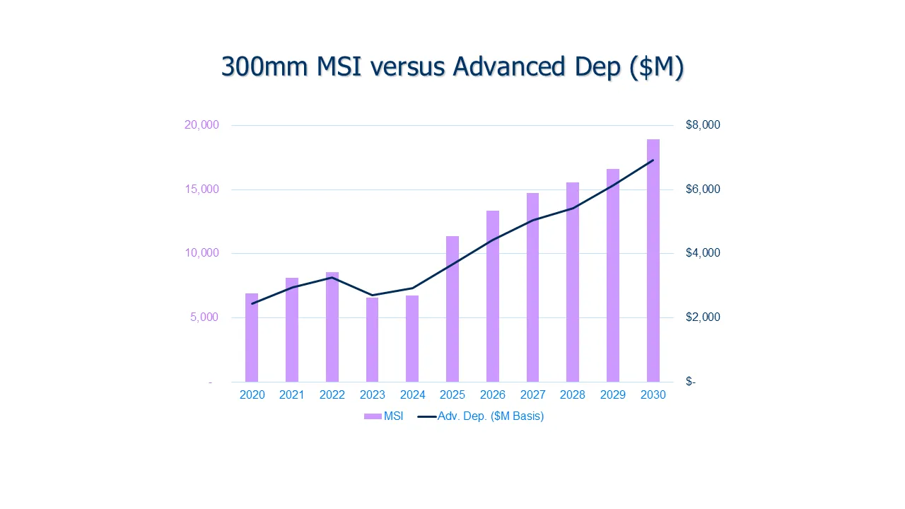
- MSI vs Advanced Dep Growth
- Technology Drivers
- Assessment of FEOL Deposition Technology
- STI/PMD
- Metal Gates
- High-κ Gate Dielectrics
- Beyond FinFet
- High Mobility Channels
- Strain
- Spacers
- Assessment of BEOL Deposition Technology
- Review of Applications
- Copper Barrier
- Copper Seed & Cobalt Seed
- ECD Copper & Cobalt
- Alternative Interconnects
- FEOL Interconnects
- Self Aligned Caps
- Low-κ Dielectrics & ESL
- Review of Applications
- Assessment of Memory Devices
- 2D & 3D NAND
- MRAM
- Cross Point/PCM
- DRAM
- Material Market Analysis and Forecasts, 2025-2030
- By Application and Year in Terms of Value and Volume:
- ALD
- CVD
- ECD
- PVD
- SOD
- By Application and Year in Terms of Value and Volume:
- Leading Suppliers & Business Assessment
- Leading Suppliers by Material
- Influence of Tool Producers
- Competitive Review
Materials covered
|
|
|
Product Information
Features
- Comprehensive Forecasting: In-depth analysis of material consumption from 2025 to 2030, segmented by technology and region.
- Technology Insights: Evaluation of key deposition technologies, including FEOL and BEOL, covering advancements like EUV and high-κ dielectrics.
- Memory Device Assessment: Detailed examination of memory technologies, including 2D & 3D NAND, MRAM, and DRAM.
- Market Analysis: Forecasts of material markets by application, including ALD, CVD, PVD, ECD, Spin-on and more, detailing value and volume.
- Supplier Landscape: Overview of leading suppliers by material and competitive assessments across segments.
Benefits
Anticipate Market Dynamics: Detailed insights into macro drivers and key demand trends for new technology adoption in the thin film industry.
Reduce Uncertainties: In-depth analysis of the shift from CVD and PVD to GAA technologies for proactive adaptation to evolving manufacturing processes.
Optimize Resource Allocation: Utilize comprehensive forecasts from 2025 to 2030 to inform investment decisions and resource distribution in critical ATF materials and technologies.
Unlock New Material Capabilities: Timely insights on advancements in high-k gate dielectrics, strain engineering, and novel DRAM structures to optimize device performance & reliability.
- Guide R&D Strategies: Leverage findings on advanced logic roadmap and patterning techniques to drive innovation & maintain a competitive edge.
Purchase
| Product | Member | Non-Member | |
|---|---|---|---|
| Advanced Thin Film Report - 1 user, One Time Purchase | $19,600 | $19,600 | Buy Now |
|
* Price is per User License. Multi-user Discounts may be available. Email [email protected] to inquire. |
* Price is per User License. Multi-user Discounts may be available. Email [email protected] to inquire.
Please review Market Intelligence License Agreement