
Current Edition:
February 2026Publication Schedule:
AnnuallyPrincipal Analysts:
Mark ThirskFormat:
PowerPoint® fileAdvanced Cleaning and Surface Preparation Report
Effective cleaning and surface preparation are foundational to advancing semiconductor technology. As the industry faces increasing challenges from material innovations, shrinking critical defect sizes, and more complex high aspect ratio features, the need for robust cleaning processes becomes even more critical. By ensuring contaminants are thoroughly removed at each stage, these processes directly impact yield and enable successful integration of new technologies, making the ongoing improvement of cleaning materials essential for the industry's continued growth.
The Advanced Cleaning and Surface Preparation Report provides a thorough exploration of these challenges and opportunities, equipping industry stakeholders with the insights necessary to align with the evolving cleaning ecosystem, improving decision-making for future planning.
Applicable to: Semiconductor Manufacturing Equipment and Materials suppliers, IDMs, Foundries, Fabless, EDA, Semiconductor IP, Design & Verification Services, other suppliers of goods and services to the semiconductor design and manufacturing ecosystem.
Market analysts, strategic and technical consulting firms, investors and investment banks. Executives, sales and marketing, business development, supply chain management, engineers, and strategic planning organizations.
Report Methodology
SEMI and Linx Consulting utilize a proven approach to these studies to gather, analyze, and validate the information required for the final reports. Key methodologies include:
Comprehensive Primary and Secondary Research
SEMI and Linx Consulting conduct field interviews with key end users, equipment makers, materials suppliers, and knowledgeable experts.
Market Modeling
Wafer start forecasts by device type and technology node are combined with detailed device architecture models to create unique forecast models for manufacturing unit operations, material demand, and market trends.
- Executive Summary
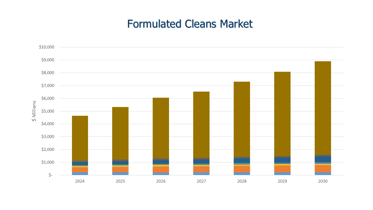
- 2024-2029 Consumption of Materials
- Growth Rates by Technology
- Forecast Drivers
- Macro Drivers
- Review Device Types
- Technology Trends by Device Type
- ASIC, DRAM, NAND, etc.
- Technology
- Semiconductor Industry Trends
- Front-end-of-Line (FEOL) Wet Cleans
- Back-End-of-Line (BEOL) Wet Cleans
- Post-CMP Cleans by Type
- Wafer-Level Packaging (WLP)
- Forecasts
- Wet and Formulated Chemical
- Volume Demand and Market, 2024-2029
- Post Etch Residue Removers
- Post CMP Cleans
- Solvents Strippers
- Selective Etches
- Supplier Analysis
- 2024 Supplier Share by Application Supplier Share Evolution
Product Information
Features
- Detailed 5-year Forecasting: Extensive coverage of key processes like Formulated Cleans, Residue Removal, Post CMP Cleans, Solvent Cleans, Selective Etches.
- In-Depth Technology Breakdown: Detailed analysis of macro drivers, device types and technology trends (ASIC, DRAM, NAND).
- Cleaning Process Insights: Comprehensive coverage from Front-End-of-Line (FEOL) to Back-End-of-Line (BEOL) web cleans, to post-CMP cleans by type.
- Supplier Analysis: Supplier shares by application, and their evolution over time.
- High-level Overview: 2024 – 2030 consumption of materials and growth breakdown by key technologies.
Benefits
Inform Strategic Planning: Detailed consumption analysis and growth trends to guide your planning and investment strategies.
Anticipate Market Dynamics: Gain insights into macro drivers and technology trends to stay ahead of competitors in the semiconductor cleaning landscape.
Capitalize on Growth Opportunities: Leverage growth rates by cleaning technology to enhance your competitive positioning, particularly in emerging device types.
Mitigate Operational Risks: Reduce uncertainty with actionable insights into key manufacturing technologies to optimize logistical planning.
Benchmark Against Industry Standards: Evaluate your market position relative to competitors through supplier analysis and insights into global footprints.
Enhance Decision-Making Confidence: Precise and dependable data insight to ensure greater accuracy in anticipating and capturing industry growth.
Purchase
| Product | Member | Non-Member | |
|---|---|---|---|
| Advanced Cleaning and Surface Preparation Report - One-Time Purchase (enterprise-wide) | $12,000 | $12,000 | Buy Now |
|
* Price is per User License. Multi-user Discounts may be available. Email [email protected] to inquire. |
* Price is per User License. Multi-user Discounts may be available. Email [email protected] to inquire.
Please review Market Intelligence License Agreement