
SEMI’s Global Executive Summit (GES) on Energy, Emissions and Efficiency, held on December 15th and 16th, 2025 took place at The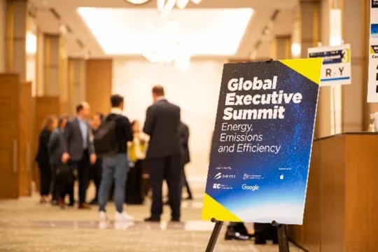 Okura Tokyo. The Summit was co-organized by SEMI and Google, with support from Apple and co-led by Dr. Saifi Usmani, SEMI Vice President of Sustainability and Bruce Gall, Strategic Partnerships Manager at Google. In addition, Microsoft and Micron helped to organize thought leader presentations and panel discussions.
The Summit was also supported by the Semiconductor Climate Consortium (SCC) and SEMI’s Energy Collaborative (EC) representing more than 110 companies spanning the semiconductor value chain. Dr. Usmani thanked the organizing team for the success of the GES and thanked the participating executives “for their commitment and collaboration to make needle-moving progress in our collective decarbonization journey.”
Abstract:
The 2025 SEMI Global Executive Summit in Tokyo convened over 150 senior executives to accelerate semiconductor industry decarbonization, moving from small-scale pilots to collective action across clean electricity, upstream materials, and gas substitution and abatement improvement. Key initiatives include a Clean Semiconductor Partnership (CSP) Pilot in Korea, enabling smaller suppliers through aggregated demand, and a coordinated approach to adopting low-Global Warming Potential (GWP) gases.
Introduction:
Ajit Manocha, President and CEO of SEMI kicked off the event, stating that “Because of AI and the quantum wave, the growth will be tremendous for the semiconductor industry. We are probably going to exceed $1 trillion in IC revenue by 2030. Thus, the time has come to recognize the need for much more collaboration among everyone here—government, industry, academia, and civil society to meet and exceed our collective net zero targets and to bring renewable energy sources into mainstream supply to lower the reliance on fossil fuels and to reduce the burden on the grid and the planet. These problems are so complex that no single company, country, or CEO can solve them alone. SEMI and Google have collaborated to create this GES platform to facilitate further collaboration at the executive levels.”
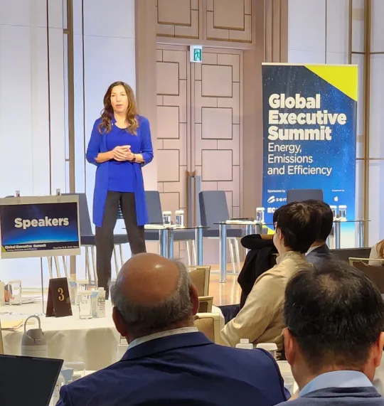 Carolin Seward, Vice President at Google opened the first day's agenda with an inspirational call to action in support of the Summit objectives. She highlighted Google's commitment to environmental ambitions by sharing "We aim for net zero emissions by 2030 and 24/7 carbon free energy by 2030. We also aim to replenish 120% of the freshwater volume we consume across our operations by 2030. Our climate ambitions are moonshots, as we recognize they may seem impossible at the time we set them, but continuing to pursue these moonshots can lead to significant and systemic change. We seek your partnership and leadership to achieve success on these moonshots.” With these inspirational words and requests for support, the Summit began.
Overview and The Responsibility of Growth
The SEMI Global Executive Summit (GES) convened more than 150 senior leaders from roughly 100 companies across 15 countries to accelerate decarbonization across the semiconductor value chain. A major topic of the Summit dialogue was the unprecedented demand driven by the rapid expansion of AI and the importance of decreasing our emissions overall. An estimated 107 new fabs are expected to come online between 2024 and 2028, with more than 30 required by 2030 to support AI-driven demand.
With this business opportunity comes a tremendous responsibility to scale sustainably. As emphasized throughout the Summit, while day-to-day business conditions evolve, we all share an obligation to maintain commitments to our respective Net Zero objectives. As Lora Ho, Senior Vice President for Taiwan Semiconductor Manufacturing Co. Ltd. (TSMC) said in her keynote, that “Driving decarbonization at TSMC is our responsibility. To achieve this, we have embedded ESG values into TSMC’s DNA and connected the critical need for decarbonization to a higher sense of purpose.”
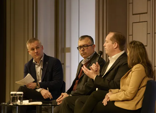
Over two days of discussions, participants reinforced the need to shift from isolated pilots to coordinated, industrywide action capable of transforming the global supply chain. The executives emphasized the responsibility to scale sustainably while maintaining commitments to Net Zero goals. The discussions centered around four main tracks-summarized below with associated calls-to-action to address the critical decarbonization challenges of our industry.
1. Fab Upstream Materials: Accelerating Supply Chain Decarbonization
The Summit participants understood that upstream materials suppliers face structural barriers such as fragmented demand from their customers, limited market leverage, and difficulty accessing clean energy procurement mechanisms such as PPAs. To address the challenge of fragmented demand for upstream emissions reductions, the Summit leaders called for all participants to send to their respective value-chain partners, a unified demand signal for emissions reduction, low carbon electricity use and transparency, in alignment with the guidelines provided in the SCC Ambition Statement, attached below. 
In addition to aligning around sending a unified demand signal, the Summit participants also aligned to issue the following calls-to-action:
Communicate and reinforce industry climate ambition by incorporating the SCC Ambition Statement (or equivalent metrics) into upcoming business reviews with top 20 suppliers.
Advance clean energy capabilities by targeted education and training programs for internal teams and key suppliers. By lowering the bar to finding trusted information on procurement-focused academies low carbon electricity courses, suppliers will be able to improve data accuracy, energy transparency, and overall decarbonization.
Support industry knowledge‑sharing by contributing company case studies to strengthen collective expertise.
Engage in coordinated energy advocacy by participating in industry-government and industry-utility discussions and provide low carbon electricity needs across the industry.
Collaborate on market‑shaping opportunities by contributing to a shared RFI process aimed at exploring participation in a buyer consortium for future PPA projects in Japan, Korea, and Taiwan.
Collaborate on large‑scale offtake demand enabling Upstream suppliers of all sizes to access low carbon electricity.
2. Clean Electricity: The Most Critical Lever for Scope 3 Reduction
Availability of low carbon electricity, labeled as ‘Clean Electricity’ for the purpose of the Summit, is the single most important factor for semiconductor Scope 3 decarbonization. This is particularly true in the APAC region which has been highlighted as one of the most challenging regions for renewable deployment due to a variety of political, financial, geographical and social factors.
The following key insights were discussed at the Asia focused clean electricity session:
- Grid reliability, long‑term market forecasts, and regulatory barriers remain major obstacles to expanding availability of low carbon electricity in Asia.
- Governments must accelerate market liberalization, invest in grid modernization, and remove permitting and interconnection bottlenecks.
- Developers and operators need to collaborate on flexible, economically viable solutions.
- Policymakers should act as catalysts, ensuring incentives and access mechanisms are effective and equitable.
Considering the above insights and challenges, the Summit participants were asked to agree to support the following calls-to-action:
- Strengthen industry advocacy by joining or renewing membership in SEMI Energy Collaborative and complementary national or regional associations to support renewable‑energy, grid, pricing, and market‑design policy work across Asia.
- Accelerate policy progress by co‑funding targeted, time‑bound policy research and analysis—such as siting reform, tariff pathways, incentive design, grid planning, and Battery Energy Storage Systems (BESS) regulatory frameworks.
- Activate internal advocacy by engaging public affairs teams to craft tailored low carbon electricity messages and participate in at least one joint industry or government engagement in 2026.
- Collaborate on the Clean Semiconductor Partnership (CSP) pilot design by participating in SEMI‑led working groups and evaluating the opportunity to act as an early anchor buyer for low carbon electricity, pending viable commercial terms.
- Promote broader adoption by supporting replication and scaling of the CSP model across other semiconductor hubs once the pilot demonstrates success.
3. GHG Substitution: Scaling Proven Solutions
 The Summit underscored the urgency of addressing high Global Warming Potential (GWP) process gases and rising Scope 1 emissions, projected to surpass Scope 2 emissions by 2041. Current efforts to pursue low GWP gas substitutions in etch and chamber clean applications remain fragmented, resulting in high material costs for high volume manufacturing (HVM) applications. While promising gas substitutions exist, the traditional paths of small scale or single customer adoption are typically too expensive due to cost scaling limitations.
With the above challenges and opportunities, the Summit participants discussed a proposal for a coordinated a fab-led, industry-wide approach to meeting cost and performance expectations:
Prioritize a single, low-GWP target gas for replacement
Co-create & execute a phased experimental plan
The over-riding thought in floating the above proposal was to enable appropriate scaling to drive cost reduction and to also accelerate adoption in ways no single company could achieve alone. With these objectives, the following calls-to-action were issued at the Summit:
- Provide Inputs: Fabs attendees to provide inputs to identify a single priority gas for replacement, including guiding the selection process of viable candidates.
- Propose Substitutes: Interested gas vendors attendees to propose substitute gas candidates that align with the priority gas for replacement.
- Co-Create Experimental Plan: Fabs, equipment OEMs and gas vendors attendees to participate in the co-creation and execution of a phased experimental plan involving low GWP gas substitution, including definition of any necessary test vehicles.
4. Abatement: Enhancing and Scaling Proven Solutions
Abatement of high greenhouse gas emissions from semiconductor manufacturing and supply facilities has the potential for rapid deployment and impact. However, the progress on deployment of advanced abatement solutions remains slow due to fragmented efforts, high costs, facility and space constraints, utility limitations, and operational complexity. Special challenges remain in deployment of abatement solutions at existing manufacturing sites due to structural, space, and utility limits thus requiring careful planning to minimize operational disruptions in production processes at these facilities.
CapEx and the Total Cost of Ownership (TCO) are other challenges, though government grants and regulatory support offer vital pathways to influence investment. Further, differences in local regulations (Point-of-Use vs. End of Pipe) drive the need for flexible, modular, and performance-based standards.
Working with these parameters, the GES attendees were challenged to determine collective solutions to addressing these fab and site-specific barriers. Industry-wide collaboration and data sharing are proven methods to unlock cross-industry deployment of new technologies. Thus, the participants explored opportunities to support high‑risk, high‑reward abatement technologies, including advanced catalytic materials, and encouraged industry‑wide collaboration and pre‑competitive R&D investment.
A major theme was the call to shift from proving concepts to proving scalability of advanced abatement solutions. Participants agreed that isolated pilots are no longer sufficient; the industry must now mobilize coordinated, global action to transform the value chain on a scale. Participants agreed to the following calls-to-action on making rapid progress on developing and deploying advanced abatement solutions:
- Collaborate on Technology Development & Evaluation:
Industry fabs and solution providers should jointly define technology readiness levels (TRLs), propose and evaluate short‑, medium‑, and long‑term abatement technologies, and share sanitized performance data to accelerate innovation. - Strengthen Industry Benchmarking & Standards:
Fabs should actively participate in SEMI SCC working groups to drive consistent, industry‑wide benchmarking, develop shared FGHG data tools and improving measurement efficiency to reduce cost and enhance accuracy. - Advance Low‑Carbon Solutions Through Coordinated R&D Funding:
Stakeholders should support government research programs (e.g., Korea's) and co‑develop a collaborative R&D funding playbook to speed progress on next‑generation catalytic and low‑carbon abatement solutions.
The SEMI Role and Next Steps

SEMI committed to sustaining momentum from the GES calls-to-action through its existing platforms including:
- The Semiconductor Climate Consortium (SCC)
- The SEMI Energy Collaborative (EC)
Executives reaffirmed support for these initiatives, recognizing them as essential platforms for shared learning, resource pooling, and coordinated advocacy.
SEMI will continue to convene stakeholders, facilitate collaboration, and drive progress on the Calls‑to‑Action established at the Summit.
Conclusion
The GES reinforced that the semiconductor industry stands at a pivotal moment. With rapid growth ahead and increasing global scrutiny on sustainability, the sector must act collectively to secure clean electricity, decarbonize upstream materials, and scale GHG substitution and abatement solutions.
Referencing the enthusiasm and the spirit of collaboration among the attendees of the GES, Spencer Low, Head of Regional Sustainability, APAC for Google said, “In ten years' time, there will be books written about the Tokyo 2025 GES and how it brought the key players together for first time to drive the collaborative decarbonization of the semiconductor industry.”
The Summit’s participants and executives set the expectation for their teams that collaboration, unified advocacy, and shared investment are key to achieving Net Zero ambitions and ensuring the industry’s long‑term competitiveness and leadership. Let us continue to deliver on these expectations!