April 14, 2025 - April 15, 2025
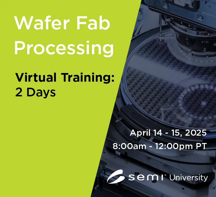
Semiconductor and integrated circuit developments continue to proceed at an incredible pace. The industry as a whole has gotten to this point of incredible complexity through the process of countless breakthroughs and developments in wafer fab processing. Today’s wafer fab contains some of the most complex and intricate procedures ever developed by mankind. Wafer Fab Processing is a 8 hour course (across two days) that offers an overview look into the semiconductor manufacturing process, and the individual processing technologies required to make them. We place special emphasis on the basics surrounding each technique, and we summarize the current issues related to manufacturing the next generation devices.
Pricing
- Members: $599
- Non-Members: $649
- Students/Vets: $549
* For group orders with 10+ attendees, and for Students/Veterans discounted pricing, please contact [email protected].
Time
8:00 am - 12:00 pm PDT
Location
United States
Course Description
By focusing on the basics of each processing step and the issues surrounding them, participants will learn why certain techniques are preferred over others. Our instructors work hard to explain how semiconductor processing works without delving heavily into the complex physics and mathematical expressions that normally accompany this discipline.
Participants learn basic but powerful aspects about the semiconductor industry. This skill-building series is divided into three segments:
1. Basic Processing Steps. Each processing step addresses a specific need in IC creation. Participants learn the fundamentals of each processing step and why they are used in the industry today.
2. The Evolution of Each Processing Step. It is important to understand how wafer fab processing came to the point where it is today. Participants learn how each technique has evolved for use in previous and current generation ICs.
3. Current Issues in Wafer Fab Processing. Participants learn how many processing steps are increasingly constrained by physics and materials science. They also learn about the impact of using new materials in the fabrication process and how those materials may create problems for the manufacturers in the future.
Learning Objectives
- Review of the semiconductor industry and its technical issues.
- Understand the basic concepts behind the fundamental wafer fab processing steps.
- Identify the key issues related to each of the processing techniques and their impact on the continued scaling of the semiconductor industry.
- Identify the basic features and principles associated with each major processing step. These include processes like chemical vapor deposition, ion implantation, lithography, and etching.
- Understand how processing, reliability, power consumption and device performance are interrelated.
- Make decisions about how to construct and evaluate processing steps for CMOS, BiCMOS, and bipolar technologies.
Who Should Attend
This course is a must for every manager, engineer and technician working in the semiconductor industry, using semiconductor components or supplying tools to the industry.
Course Topics
- Raw Silicon Wafers
- Ion Implantation
- Thermal Processing
- Contamination Monitoring and Control
- Wafer Cleaning and Surface Preparation
- Chemical Vapor Deposition
- Physical Vapor Deposition
- Lithography
- Etch
- Chemical Mechanical Polishing
- Cu Interconnect and low-k Dielectrics
- Leading Edge Technologies and Techniques
- ALD
- High-k gate and capacitor dielectrics
- Metal gates
- SOI
- Strained silicon
- Plasma doping
Instructor

Chris Henderson
Semitracks, Inc.
Important Information
Note that only the person who registered will receive a certificate of completion. This virtual training will not be recorded. Attendees must be present to access course knowledge.
Can't find the training link day of? After you register, you will receive the link to the live training via the email address you provided. In addition, you will receive email reminders about 24 hours in an advance and an hour before with the same link. Please keep these emails on hand to access the trainings on time. If you do not see any confirmation emails, please check your junk/spam folders before contacting SEMI U for support.