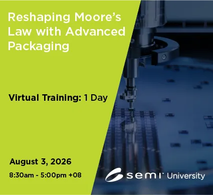
August 3, 2026
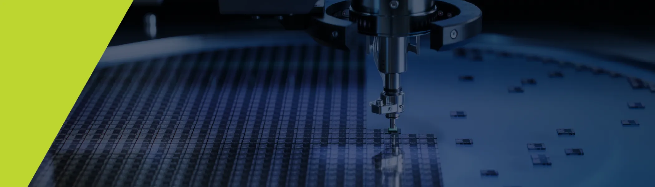
As transistor scaling slows under the physical limits of lithography, the semiconductor industry is entering a new era-one where innovation is driven not just by node shrink, but by how chips are integrated and packaged.
Pricing
- Members: $599
- Non-Members: $649
* For group orders with 10+ attendees, and for Students/Veterans discounted pricing, please contact [email protected].
Time
8:30 am - 5:00 pm +08
Location
Singapore
Course Description
This workshop explores how advanced packaging is redefining the trajectory of Moore's Law. Participants will gain insight into cutting-edge approaches, such as heterogeneous integration and chiplet architectures, that enable continued performance growth beyond traditional scaling limits.
We will delve into key packaging, including wafer-level packaging, fan-out wafer and panel-level solutions, 3D integration, and embedded packaging- highlighting how each enhances transistor density and system performance, along with the associated technical challenges. The session will also cover next-generation interconnect and bonding techniques, including thermocompression and hybrid bonding used in advanced die-stacking solutions such as SoIC-X and SoIC-P.
In addition, the workshop will examine evolving interposer architectures (2.1D, 2.3D, 2.5D, and beyond), including platforms such as CoWoS-S, CoWoS-L, and CoWoS-R. It will also explore emerging interposer materials like glass substrates, covering their benefits, fabrication processes, technical challenges, and supply chain landscape in supporting the continued evolution of Moore's Law.
Who Should Attend
This course is intended for both manufacturing and R&D know-how in IC packaging professionals, including but not limited to:
- Directors
- Managers
- Process Engineers
- R&D Engineers
- Sales and Application Engineers who supply packaging materials and tools
Learning Objectives
- Understand the principles in the evolution of IC packaging and how the semiconductor industry has evolved with time.
- Understand the principles of Interconnections ranging from TAB, and Wirebond to various Flip Chip bonding, such as thermocompression bonding with NCP, C4, ACF for manufacturing and R&D development.
- Review the interposer of leadframe, ceramic, flex to BT substrates for Microelectronics packaging.
- Explain the assembly flow and new assembly techniques from backgrinding to singulation.
- Describe the material characterization from bulk to interfaces to reduce stress and enhance interfacial adhesion for reliability enhancement.
Course Topics
- Advanced packaging and material characterization.
- Packaging principles and how packaging evolves into heterogeneous packaging.
- Packaging concepts such as Fan-in, Fan-out WLP, Embedded packaging technology, 3D packaging, TSV.
- Wirebond and Flip chip interconnect technologies inclusive of interposer technologies, such as leadframe, ceramic, flex and substrate.
- Assembly processes from backgrinding to singulation for QFP and FBGA packages.
- Material characterization to select materials to reduce stress and strengthen the interface for reliability enhancement.
Instructor
Dr. Lee Teck Kheng
Institue of Technical Education
Important Information
Note that only the person who registered will receive a certificate of completion. This virtual training will not be recorded. Attendees must be present to access course knowledge.
Can't find the training link day of? After you register, you will receive the link to the live training via the email address you provided. In addition, you will receive email reminders about 24 hours in an advance and an hour before with the same link. Please keep these emails on hand to access the trainings on time. If you do not see any confirmation emails, please check your junk/spam folders before contacting SEMI U for support.