June 11, 2025

Hosted by SEMI MSIG
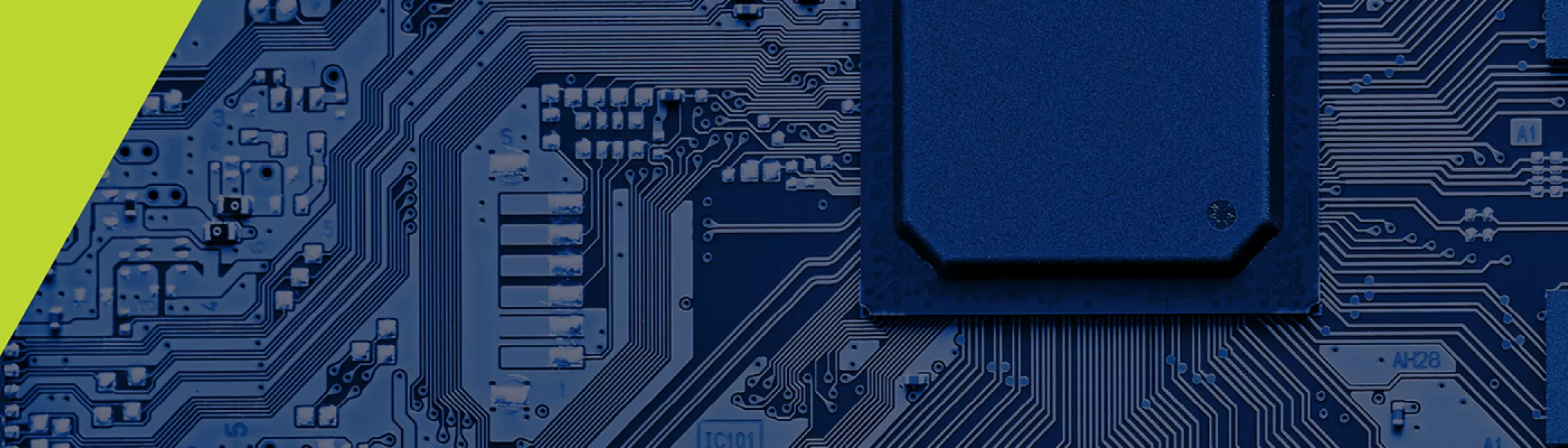
Innovative Lab to Fab Semiconductor Processes: Advancing sensing, smart manufacturing, and biomedical applications
Emerging MEMS and sensor technologies demand both advanced process capabilities and robust pathways to volume manufacturing. NOEL Technologies, a Silicon Valley MEMS foundry, brings decades of expertise in microfabrication – from state-of-the-art lithography and deep etching to thin-film deposition and multi-layer integration. Its versatile fabrication facility supports wafer diameters ranging from 50 mm up to 300 mm, enabling prototyping on small substrates as well as scale-up to full 300 mm production. NOEL’s engineers excel at integrating novel materials and processes to create structures that often lack a conventional manufacturing path, while handling complex builds with multiple mask layers with both wet and plasma etching of silicon, dielectrics, and metals. Through a proven “Lab-to-Fab” approach, NOEL serves as a vital bridge from R&D to high-volume fabrication, accelerating the transition of innovative designs from the laboratory to the fab floor.
Recent collaboration through Pure Wafer’s acquisition of NOEL Technologies has further expanded these capabilities. Pure Wafer, a leading U.S. provider of high-purity silicon wafer solutions, adds in-house supply of prime silicon substrates (50 mm–300 mm) and an extensive portfolio of exotic dielectric and metal thin films. By coupling NOEL’s proprietary MEMS processes with Pure Wafer’s materials expertise, the combined team delivers a “complete silicon solution” that enhances device performance and yield for next-generation sensors. This synergy is enabling cutting-edge sensor technologies in IoT, biomedical, and industrial applications, supported by faster prototyping cycles and a streamlined path to market. Equally important, the integration provides key business advantages – from cost efficiencies via comprehensive on-shore services (e.g., wafer reclaim and reuse) to improved supply chain resilience through a domestic source for critical materials and fabrication.
This presentation will showcase how the NOEL–Pure Wafer partnership supports next-generation sensor innovation in alignment with the key industry tracks driving future advancements in IoT, Intelligent Sensing, Advanced embedded system Technologies, Multi-Sensor capabilities, Smart Manufacturing, and biomedical applications. By leveraging Pure Wafer and NOEL Technologies' expertise, MEMS and sensor innovators can achieve superior device performance, faster prototyping, and scalable production solutions. This collaboration is paving the way for next-generation innovative sensing solutions that drive technological breakthroughs across industries.
Time
8:00 am - 9:00 am PDT
Location
United States
Ardy Sidhwa, Ph.D., CTO, Noel Technologies

Dr. Sidhwa has over 25 years of innovative contributions to semiconductor device manufacturing and processing development. His expertise includes Mergers and Acquisitions, Semiconductor processing and characterization, Nanotechnology, R&D, Capital equipment sourcing, Devices Characterization and Yield Enhancement, Semiconductor Fab constructions, Semiconductor silicon wafer reclaim, Equipment parts cleaning using novel surface cleaning methods, Lean manufacturing, Quality control, Materials characterization, Sustainability, Design of Solar Cells and Composite Armor Manufacturing for the US government. In addition, he is proficient in technology development for strategic alliances and multiple joint ventures. Dr. Sidhwa has 7 U.S. patents issued, two pending applications in multidisciplinary fields, and over 100 publications.
Dr. Sidhwa has led teams to successfully deliver numerous technologies through a complete product development lifecycle, from early R&D to end customer deployment and qualification. He excels at troubleshooting endemic technical manufacturing process integration and reliability issues through systematic and thorough investigation. His hands-on problem-solving skills have repeatedly been demonstrated at startups and established companies by rapidly delivering qualified products to the market.