
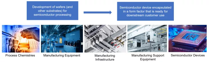
Semiconductor Manufacturing Process
The Semiconductor Manufacturing Process includes all the direct and indirect equipment and materials required to manufacture semiconductor "chips" and similar devices such as solar panels, light emitting diodes (LEDs), flat panel displays (FPDs), semiconductor sensors, and microelectromechanical systems (MEMS).
Semiconductors Enable Everything Digital and Shape the Modern Society
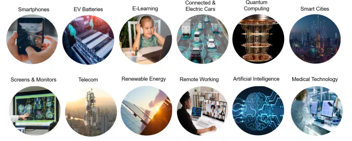
Semiconductor technology development and production fuels future economic growth in artificial intelligence, machine learning, autonomous driving, cloud and edge computing, high-performance computing, 5G, smartphones, and more.
This Explainer was developed by the SEMI PFAS working group and is maintained under their oversight.
This guide aims to be as clear and concise as possible, while also explaining some of the important, but finer points in the PFAS discussion with sufficient detail. In the interest of making this information available as quickly as possible, some organizational clarity may have been sacrificed. The working group plans to restructure this information in the next few months to assist comprehension. If you have any concerns about the information on this page, or would like to offer some additional ideas for it, please contact [email protected]
Please note: SEMI makes no warranties or representation to the accuracy or usefulness of the information contained on this webpage. Accuracy is solely the responsibility of the user. Users are cautioned to refer to other relevant literature of the subject matter herein. This information is subject to change without notice. This "explainer" was developed by members of the SEMI PFAS Working Group. Please send suggestions for improvement to [email protected]