
July 15, 2026
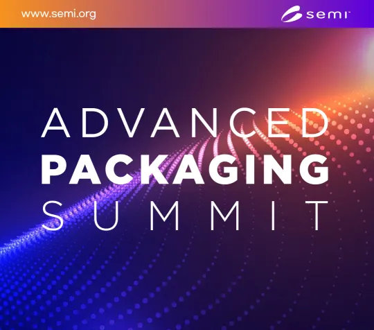
Advanced Packaging Summit 2026, under the theme “Packaging the Future of AI – From Silicon to Photon,” will examine the evolution of packaging technologies in the AI era and their broader implications for the semiconductor industry. Featuring presentations by leading industry experts, the summit will explore market shifts driven by the growing demand for AI semiconductors, along with key technologies enabling advanced packaging. The program will also highlight the innovation journey from silicon-based integration technologies to photonics-based interconnects, which are essential to enhancing packaging productivity and scalability. Panel discussions in each session will further provide opportunities to exchange insights on real-world applications, technical challenges, and possibilities for cross-industry collaboration, while exploring new business opportunities and strategic perspectives created by advanced packaging technologies in the AI era.
Time
8:30 am - 5:00 pm KST
Location
Convention Hall 1, 3F, Suwon Convention Center South Korea
South Korea
OVERVIEW
- Date: July 15(Wed), 2026
- Time: 08:30 - 17:00
- Venue: Convention Hall 1, 3F, Suwon Convention Center
- Language: Korean/English (Simultaneous interpretation will be provided)
- Organizer: SEMI Korea
SPONSORS
 |  |  |
 |  |  |
 |
NOTICE
- The agenda is subject to change at the discretion of the speakers.
- Presentation files agreed by speakers will be provided to attendees after the event through SEMI registration website.
CONTACT
- SEMI Korea Program Team ([email protected])
Agenda
Welcome Reception


2026 Outlook for the Advanced Packaging Industry
Making 3DIC Manufacturable for AI: From Vertical Integration to Scalable Production
As AI systems push requirements for higher bandwidth, lower power, and increased integration density, 3D integrated circuits (3DIC) are moving rapidly from development to production. However, scaling 3DIC introduces complex application challenges across the manufacturing flow, where process interactions and control become critical.
This talk examines key 3DIC applications and process challenges, including high aspect ratio TSV etch, void free TSV fill, and dielectric deposition, required for reliable wafer and die level stacking. Emerging applications such as inter die gap fill for advanced chiplets integration and plasma dicing for improved yield, edge quality, and die strength further increase integration complexity and productivity demands.
The presentation highlights Lam Research innovations across etch, deposition and clean processes that enable tighter process windows, improved uniformity, and higher throughput. In addition, equipment intelligence and data driven control are increasingly essential to enhance yield learning and manufacturing productivity. Together, these advances are enabling scalable, high volume 3DIC manufacturing for next generation AI systems.

Advanced Packaging: Enabling AI at Scale
The future of compute will not be defined by silicon alone. As AI reshapes industries and economies, advanced packaging has become the foundation of the next era of innovation, enabling unprecedented gains in performance, efficiency, and scale. During his keynote, Yin Chang will explore how breakthroughs in heterogeneous integration, chiplets, and advanced manufacturing are transforming bold AI ambitions into deployable systems, and why AI leadership will depend not only on compute power, but on the ability to integrate and manufacture at scale.

Advanced Power Module Packaging Technologies
The rapid electrification of automotive and industrial systems is placing increasingly stringent demands on power semiconductor devices in terms of voltage capability, thermal performance, reliability, and system integration. This presentation reviews recent trends in power devices and power module packaging technologies aimed at improving performance while addressing cost and manufacturability constraints.
First, the fundamental differences between digital and power devices are outlined, followed by an overview of power device applications based on silicon (Si), silicon carbide (SiC), and gallium nitride (GaN) technologies, together with Amkor’s product portfolio.
Next, power module packaging technologies are discussed with a focus on key electrical and thermal challenges. Representative solutions, including advanced interconnects, cooling architectures, and embedded power modules, are introduced, along with a brief overview of Amkor’s technology roadmap.
Finally, the role of the Amkor Technology Japan R&D Center in supporting open innovation and global collaboration is briefly discussed.
Networking Break
Panel Discussion
Lunch

Advanced Packaging Technology for AI/HPC
The presentation explores advanced packaging technologies designed to meet the escalating performance and power efficiency demands of AI and High-Performance Computing (HPC). To overcome the limitations of traditional semiconductor architectures, System Technology Co-Optimization (STCO) is introduced as a critical framework for managing thermal crosstalk and enhancing heterogeneous integration. The discussion highlights key innovations, including Customized HBM (cHBM) for optimized base-die performance and Samsung's 2.xD packaging portfolio, which encompasses Cube S, Cube E, and Cube R. Specifically, the 2.3D Cube E leverages panel level packaging to enable larger interposers and increased HBM integration, significantly improving productivity and reducing silicon fab burdens. The technical achievements in PLP—such as precise warpage control and the realization of fine RDL patterns (2/2μm)—are detailed to demonstrate their viability for large-scale AI chips. Furthermore, the roadmap extends toward 3D integration and Co-Packaged Optics (CPO) to maximize bandwidth and energy efficiency. Finally, the importance of an ecosystem-wide collaboration is emphasized as the driver for future innovation in "More than Moore" technology. These advancements collectively provide a scalable path toward the next generation of AI hardware acceleration.
Latest Development Status of Glass Core Build-up Substrate
Glass core substrates exhibit low CTE and significantly higher rigidity than conventional organic substrates and are therefore regarded as promising core materials for next-generation build-up packages. However, a major challenge lies in the occurrence of SeWaRe defects (delamination in glass), which arise from thermal stresses induced by the mismatch in the coefficients of thermal expansion (CTE) between the glass material and the build-up resin.
To mitigate this issue, we proposed a structure in which the corner regions of each individual piece are formed from resin. However, considering the thermal history during chip mounting, it became evident that the suppression effect was insufficient. Therefore, an edge‑protection material was applied to relieve the stress concentrated at the edges of each individual piece. As a result, it was confirmed that SeWaRe defects could be effectively suppressed even under thermal loading.
Through these efforts, we successfully developed a glass core build-up package substrate incorporating 11 layers of single‑sided copper wiring (22 layers in total).

Beyond Moore's Law: How Silicon Photonics and Advanced Packaging Are Redefining HPC
AI and data-intensive workloads are outpacing what conventional semiconductor technology can deliver. Two innovations are stepping in to close the gap: Silicon Photonics, which brings optical-speed, low-power data transmission into the data center, and Advanced Packaging, which uses chiplets and 2.5D/3D integration to maximize performance and efficiency at the chip level.
This talk examines how these complementary technologies are reshaping HPC architecture—covering their current state, how they work in tandem, and the key technical and commercial barriers to large-scale adoption.

CPO Packaging: Challenges and Opportunities
Co-packaged optics (CPO) is emerging as a key enabler for scaling bandwidth while containing power and cost in next-generation AI and cloud infrastructure. By moving optical engines closer to the switch ASIC and shortening high-speed electrical reaches, CPO can reduce SerDes power, ease signal-integrity constraints, and increase overall front-panel bandwidth density. However, delivering these benefits at volume requires new approaches across package architecture, manufacturing, and system integration.
This presentation reviews the main packaging challenges that must be solved to industrialize CPO, including thermal management and heat spreading near high-power silicon, fiber attach and optical alignment tolerances, photonics/laser integration choices, high-density optical and electrical I/O, substrate and interposer selection, and reliability risks such as warpage, CTE mismatch, and contamination control. Test and rework strategy, yield learning, and supply-chain readiness (materials, assembly, and metrology) are highlighted as practical barriers to adoption.
The talk also outlines opportunities created by CPO packaging innovations—such as modular optical tiles, standardized fiber interfaces, advanced lid/heat-sink concepts, and co-design of electrical, mechanical, and optical domains—to unlock higher radix switches and lower system power. Attendees will leave with a structured view of technology tradeoffs, a roadmap of near-term versus long-term packaging options, and actionable considerations for bringing CPO from prototypes to deployable products.
Networking Break
Panel Discussion
Registration

※ Early-bird Registration Deadline: July 8 (Wed), 2026, 17:00 PM (KST)
| Early Bird | On-site | Group | |
| SEMI Member | KRW 308,000 | KRW 385,000 | KRW 275,000 |
| Non-Member | KRW 363,000 | KRW 330,000 |
※ Group registration fee applies to groups of five or more from the same company.
※ For group registration inquiries, please contact SEMI Korea Program Team at [email protected].