downloadGroupGroupnoun_press release_995423_000000 copyGroupnoun_Feed_96767_000000Group 19noun_pictures_1817522_000000Member company iconResource item iconStore item iconGroup 19Group 19noun_Photo_2085192_000000 Copynoun_presentation_2096081_000000Group 19Group Copy 7noun_webinar_692730_000000Path
Skip to main content
Default Banner Image

SEMICON West

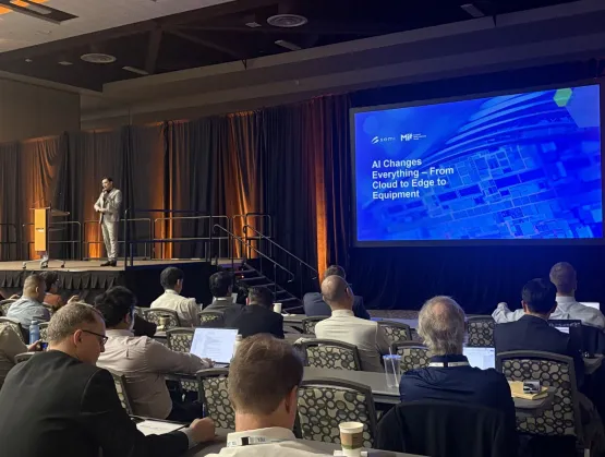
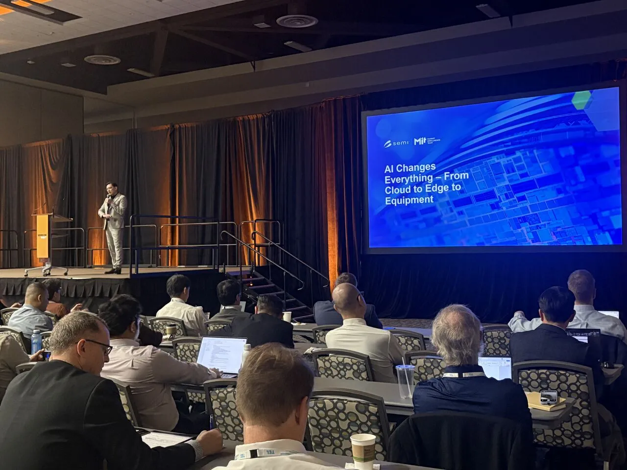
The 2025 SEMICON West Market Symposium brought together leading analysts and strategists to decode the powerful forces shaping the global semiconductor market. Building on last year’s focus on fabless growth and workforce initiatives, this year’s sessions centered on the rising influence of geopolitics, trade policy, and AI-driven investment. Experts from SEMI, Integrated Insights, Boston Consulting Group, Kearney, PwC, WSTS and TechSearch shared perspectives on how global shifts from tariffs to technology races are redefining supply chain resilience and regional competitiveness.On October 6 in Phoenix, Arizona, Clark Tseng, Senior Director of SEMI Market Intelligence, hosted the symposium and presented along with industry experts on the current trade environment from various angles. Discussions ranged from the effects of U.S. tariffs across the globe, to sector-specific considerations and market growth areas. US Trade Dynamics in Semiconductors As the geopolitical landscape in the U.S. becomes more complex, Iacob Koch-Weser, Associate Director, Global Trade Investment at Boston Consulting Group outlined the impact that tariffs are having on the U.S. industry. The average American tariff, he said, is higher than any time in the last 75 years. Although the semiconductor industry is less affected by high tariffs than other sectors, Koch-Weser noted that might change with the administration’s expanded Section 232 Tariff that imposes 50% tariffs on steel, aluminum, and their derivatives on nearly all trading partners. To explain, he described four potential Section 232 tariff scenarios, underscoring limited Section 232 enforcement as the ideal approach.Tariffs may be deprioritized in favor of chips incentivesThere may be targeted carveouts for alliesThe administration may impose high tariffs with limited exceptionsThere may be a 100% tariff rate To cope with tariff uncertainty, Koch-Weser recommended that companies consider reshaping policies, mastering trade compliance, and reconfiguring supply chains if possible. He also shared four potential outcomes for the future of U.S. trade that could take effect within the next 18-24 months. The U.S. may run its own system while the rest of the world aligns to World Trade Organization (WTO) rules.North American countries may form a stronghold, leaving all other countries to choose between the North American alliance and WTO standards.Countries may form new blocs and preferential agreements, creating multiple economic spheres worldwide.Global cooperation could break down, forcing countries to fend for themselves.With everything considered, he reinforced that the U.S. is still an attractive place for semiconductor investment. The current administration, he said, recognizes the importance of bringing advanced technologies back to the U.S. Navigating Uncertainty: AI-Driven Growth and the U.S. Semiconductor Manufacturing RenaissanceContinuing discussions on tariffs, SEMI’s Clark Tseng painted a picture of the current U.S. semiconductor industry. He divided his presentation into four key areas: near-term economic uncertainty, AI changes everything, semiconductor market equipment forecast, and material market outlook.Near-term economic uncertainty: U.S. tariff policies are contributing to inflationary pressures and altering global trade patterns, leading to cross-border uncertainty that is slowing investment. U.S. tariff revenue, he said, has expanded from $7 billion in January 2025 to $29.5 billion by August, forcing companies to sacrifice margins to compensate. AI changes everything: By 2030, Tseng noted that nearly half of the semiconductor industry’s capital expenditure will be driven by AI, pointing to sustained growth in AI-driven cloud infrastructure spending through 2028 forecasts. AI is also moving beyond data centers into edge computing and endpoint devices.Semiconductor market equipment forecast: Tseng reported that the outlook for the equipment market remains strong over the next three years. However, the biggest risk to the market is a potential slowdown in AI investment and adoption. Additionally, U.S. export controls and changes in regional supply chains present some challenges. Last year, China was the largest market for semiconductor equipment, but Tseng expects continued normalization amid broader market adjustments. Taiwan and South Korea experienced the strongest year-over-year growth, driven by demand for AI chips and high-bandwidth memory (HBM). Material market outlook: Silicon wafer shipments grew strongly in Q2 of 2025, but Tseng flagged this as unexpected and cited tariffs as a possible explanation. He noted the 300mm wafer segment is expected to grow 7% in 2025, while 200mm is projected to decline. The total wafer material market, he said, is also expected to grow by 6% this year. Additionally, wet chemicals experienced a 16% expansion in 2025, while silicon wafers, photolithography materials, and CMP materials are in recovery. Semiconductor Market – Status Outlook Tobias Pröttel (or Proettel), CEO of World Semiconductor Trade Statistics (WSTS), reported that the industry’s rebound remains firmly on track, with the latest WSTS statistics confirming a 19% year-over-year increase in global semiconductor sales during the first half of 2025. Total revenue reached $346 billion over the period, supported by strong demand for AI-driven infrastructure and next-generation data centers. Based on this solid first-half performance, WSTS has raised its full-year 2025 forecast to $728 billion, representing 15% annual growth, and now expects the market to reach around $800 billion in 2026, keeping the industry on course toward the $1 trillion milestone before the decade’s end.Logic and Memory continue to lead the expansion, driven by GPUs, AI accelerators, and high-bandwidth memory (HBM), while other product categories are showing steady recovery after the recent downturn. Pröttel noted that this growth is not confined to a single region: the Americas, China, and Asia Pacific are all posting double-digit gains, reflecting strong global momentum across the semiconductor value chain.Strategic Approaches to Semiconductors by Major Economies Following Pröttel, Kearney’s Vice President, PERLab, Sanjay Kumar outlined the semiconductor investment climates in South Korea, Japan, Taiwan, and India. South Korea is currently focused on maintaining its lead in memory, diversifying into logic, localizing its supply chain, developing advanced packaging capabilities, and investing in startups. Kumar also noted the Korean approach of offering loans, as opposed to the U.S. strategy of providing direct grants. In addition, Kumar said the Korean government plays an active role in how it wants its companies to grow, whereas the U.S. takes a more passive approach in this regard.Japan is also honing its leadership in key areas like materials and memory, and Kumar also pointed to the country’s efforts to build additional advanced packaging capacity. Japan, he said, aims to grow its industry though a mix of grants, loans, and tax credits. Among the country’s notable subsidies include a 50% subsidy for TSMC – its largest so far – as well as a $4 billion subsidy for Rapidus. Taiwan’s semiconductor industry is critical for protecting its national security. As a region with limited land, power, and water, Kumar noted that Taiwan is currently focused on developing its talent base. Its government is offering tax credits for R D and equipment and up to a 50% cost share for R D projects. India, he said, has one of the most ambitious incentive programs in the world. Through its India Semiconductor Mission (ISM), the country offers a 50% federal subsidy, in addition to a 20-30% state subsidy in its quest to cover the entire semiconductor ecosystem. Kumar also spotlighted some of India’s successes – like the joint venture between Renesas, CG Power and Industrial Solutions, and Stars Microelectronics – to build a new OSAT facility.Adapting to New Policy and Navigating the U.S. Semiconductor Landscape – Insights from Taiwan Taiwan is a critical trade partner of the U.S., ranking fourth in total trade volume as of July 2025. With Taiwan’s stronghold on the U.S. chip ecosystem, Paul Poliakov, Senior Manager, International Tax Services, CPA at PwC Taiwan detailed both the bottlenecks and developments regarding Taiwan companies’ investments in the U.S. Among the investment bottlenecks he highlighted were higher costs of building facilities in the U.S., multiple layers of compliance requirements that may be intimidating for new market entrants, and complex visa and tax regulations. In addition, Section 232 investigations on semiconductors are ongoing, with several potential policy changes that could take effect. The pending United States-Taiwan Expedited Double-Tax Relief Act could help ease burdens, he said, but it has yet to pass in the U.S. Senate as of October 2025. If it passes, it will integrate benefits for Taiwanese individuals and businesses into the U.S. tax code, which could substantially benefit Taiwanese investment in the U.S., including manufacturing, services, distribution, and a wide variety of other industries. Furthermore, Poliakov suggested that businesses maintain flexibility in their investment strategies, engage with U.S. state and local governments that can offer investment incentives, and work with professionals to ensure regulatory compliance. Geopolitical Shifts in Advanced Packaging AssemblyIn the final presentation of the 2025 Market Symposium, Jan Vardaman, Founder and President of TechSearch International provided an overview of the current advanced packaging market. Although advanced packaging represents the highest growth area in the industry, Vardaman highlighted that packaging complexity is also soaring. R D, testing, and equipment support infrastructure, she said, are becoming more critical for meeting future packaging needs. Even though assembly is mostly done in Asia, new U.S.-based advanced packaging facilities from Amkor, TSMC, and others represent signs of change. Still, Vardaman noted that the U.S. has almost no capability to produce advanced IC substrates using build-up film, which are needed to support high density applications. In addition, she highlighted that building more silicon fabs on U.S. soil won’t solve its national security or supply chain concerns.For the U.S. to create a sustainable packaging ecosystem, Vardaman concluded that support of assembly facilities is crucial. Ultimately, businesses must be willing to pay more for U.S.-based packaging in favor of potential supply chain resilience and national security benefits. SEMI would like to thank all speakers, sponsors, and attendees for the success of this year’s Market Symposium. Explore the latest SEMI Market Intelligence reports, covering historical reporting, actionable foresight into emerging trends and technology investments to make confident, forward-looking decisions across the semiconductor and microelectronics value chain.Clark Tseng is Senior Director, Market Intelligence Team at SEMI. Nishita Rao is Director, Product Marketing at SEMI.
Read More
SEMICON West in Phoenix, Arizona, will bring together all of the SEMI Sustainability efforts and programs under one roof over three days. With back-to-back sessions from October 7-9, this year’s Sustainability EHS Program will offer expert insights on the most pressing sustainability topics facing the microelectronics industry. Tuesday will kick off the program and focus on the business aspects of driving to sustainability in the semiconductor sector. On Wednesday, the Pavilion hosts discussions on water risk, water management, circular economy solutions and the needs for innovation from startups. Finally, Thursday will highlight the current emissions landscape, milestones and achievements, and solutions developed by the SEMI Semiconductor Climate Consortium (SCC). The 2025 event also marks the first public discussions of the full scope, findings and status of the SCC’s direction.All three days of the Sustainability EHS Program are sponsored by Edwards, Schneider Electric, TEL, SCREEN, Sundt and the Greater Sacramento Economic Council. Here’s a sneak peek at what the 2025 program has to offer. Registration for SEMICON West is open.The Business of Sustainability – Tuesday, October 7 Sustainability Panel: Path to Success Sustainability hits the keynote stage with Tuesday afternoon with a panel discussion detailing a plan for meaningful sustainability progress. The panel, titled Sustainability Panel: Path to Success—The Semiconductor Industry Leads the Way for a Resilient Future, will take place on the CEO Summit Keynote Stage from 2:35-3:35 p.m. Experts from Applied Materials, BASF, Micron, Google, and Qualcomm will cover strategies on how collaboration, supplier engagement, and clean technology investments are reducing emissions and propelling the industry closer to its sustainability goals. Attendees will discover what’s working, what’s still to come, and how the industry will forge its way toward a more sustainable future.A Musical Performance by Ay YoungIn anticipation of the Path to Success panel discussion, Tuesday will also spotlight an exciting musical guest. AY Young is a singer, songwriter, and the founder of the longest-running clean energy concert series in the U.S. At 2:20 p.m., he’ll take to the CEO Summit Keynote Stage for a memorable performance and give a glimpse into how important sustainability has become to attract a new generation of talent. Through his musical talent and deep commitment to clean energy, Young was appointed as a United Nations (UN) Young World Leader in 2020, helping the organization further its 17 Sustainable Development Goals. His Project17 initiative is a 17-song album, with each song centering on a different goal and backed by a corporate sponsor that aligns with it. Young will also attend the Sustainability Reception from 5-6:30 p.m. at the Sustainability Pavilion Theater.EHS Regulatory OverviewThe wide range of regulatory topics will be showcased in the first session on Tuesday at the Sustainability Pavilion. Expert speakers and advocacy groups will deliver key insights on the threats and challenges, and the research and collaboration opportunities currently at play in the regulatory environment, with special focus on keeping electronics manufacturing strong. Climate Equity Social Impact Workgroup (CESI) Aligning with the theme of the UN Sustainable Development Goals, the SEMI Climate Equity Social Impact (CESI) Working Group will highlight how its members are progressing real-world outcomes for climate, education, and global cooperation. This session will run from 3-4 p.m. at the Sustainability Pavilion Stage, and it’s ideal for anyone in the industry who’s passionate about sustainable partnerships. Innovations Enabling Reduce, Reuse, Repurpose and Recover – Wednesday, October 8Resource Use and Circular EconomyWednesday’s 10:15-11:30 a.m. session, Resource Use and Circular Economy will offer tactical solutions to help fabs reach up to 80-90% circularity. The goal of this session is to lay a foundation for transforming the industry’s circularity concerns into practical opportunities, which will be achieved over two panel discussions. Discussion 1, A Circular Value Chain: Challenges and Leading-Edge Solutions, will highlight solutions for eliminating waste and reducing manufacturing costs through circular technologies. This panel will feature experts from Edwards, Syensqo, and ElectraMet and will be moderated by Subgeni’s Taimur Burki. These subject matter experts will highlight their company solutions, but also other areas they see in need of consideration from a circularity lens, as well as best known practices across fabs. Water is a precious resource, and how the industry manages it is crucial for its long-term success. Discussion 2, Tactical Maturity Scales for Water Management, will unveil two new guides developed by SEMI’s Water Management Working Group. Both products are designed to move manufacturers from both large and small fabs and manufacturing operations to assess their water needs and most efficiently improve water reuse by up to 80%. This panel will be led by speakers from Aquatech, SCREEN, Sundt, Ovivo, and C2MI. Water Resilience Starting at 11:30 a.m. at the Sustainability Pavilion Stage, attendees will hear from the SEMI Environmental Risk Mitigation and Reporting Working Group lead - Senior Sustainable Program Manager – Alua Suleimenova – as she shares her insights and findings from a recently completed study by WaterPlan on industry water risks within the semiconductor value chain. The topic and findings will then be addressed by a panel, where Suleimenova will engage leaders from ASM, Waterplan, ERM, and the Alliance for Water Stewardship, in a conversation about water, nature, and associated corporate risks. Although companies are making strides to protect water access, it’s becoming clear that a focus on internal activities will not move the needle significantly enough for achieving long-term resilience. This panel will offer solutions for adapting water-related risks to the supply chain, with a focus on North America, Asia Pacific, and Europe.Other Wednesday AttractionsSEMI S3 – Startups for Sustainable Semiconductors: SEMI S3, or Startups for Sustainable Semiconductors, is an annual program by the industry’s venture capital divisions designed to boost awareness of semiconductor industry needs by inviting promising startups to be mentored and pitch their solutions to our industry. Earlier this year, 145 candidates submitted applications. Now, it’s down to 15 finalists, who will present at SEMICON West from 2-4:40 p.m. at the Sustainability Pavilion, following a Fireside Chat from experienced innovation experts from 1-2pm.Accelerating Sustainability with Smart Manufacturing – Presentations Poster Session: Technical papers and posters focused on sustainability solutions – from water to energy – will also be presented in the Smart Manufacturing Pavilion from 2-5:15 p.m., providing an opportunity to network with industry leaders and discover the latest best practices for how machine learning and AI can reduce water and waste in fabs.Reducing Emissions – Thursday, October 9SCC – Tackling Emissions Across the IndustryExpect a full-house at Thursday’s all-day session featuring SCC – Tackling Emissions Across the Industry. From 10:15 a.m. to 3:00 p.m., the SEMI SCC leaders and experts will detail its findings and projects addressing the industry’s emissions. SCC has been focusing on ensuring consistent and measurable progress in decarbonizing from 2021 levels. Key topics include: Reporting and aligningBaseline, ambition, and roadmapAbatementLow Global Warming Potential (GWP) gases workLow Carbon Economy (LCE) access and procurementEnergy efficienciesScope 3 upstreamSEMICON West also features SEMI U courses to learn more about sustainability in our industry. For example, on Thursday, SEMI U: PFAS Compounds in Semiconductor Environment, is being offered from 8 a.m. to noon. This course is available for purchase. Support the SEMI Forest community effort to reforest our planet by funding a range of certified carbon avoidance and tree planting projects. Our goal for SEMICON West is to fund planting for 100,000 trees. Scan the QR code below to contribute and help us meet our goal.Learn more about the 2025 SEMICON West Sustainability EHS Program. Follow SEMI Sustainability on LinkedIn for regular updates on sustainability initiatives. Saifi Usmani is Vice President for Sustainability at SEMI.
Read More
The SEMI Startups for Sustainable Semiconductors (S3) program announced 15 startups chosen as finalists for pitching to the industry at SEMICON West 2025 in Phoenix, Arizona. The finalists were chosen from a field of 35 semifinalists after a virtual pitch event over 2 days. Startups were evaluated by the organizing committee on five factors: the sustainability impact on our industry, commercial viability of product, company value proposition, the quality of the pitch and the startup team.The committee, made up of experienced Corporate Venture Capitalists (CVCs) from the global semiconductor industry, initially received 145 submissions in all three categories identified for 2025:Sustainable Semiconductor ManufacturingSustainable Data CenterGen AI for Sustainable DesignNow in its 4th year, the program features strong exposure to semiconductor industry CVCs, through the personal mentoring each startup receives. Mentoring topics are tailored to align with the needs and strategic positioning of the startup business plan, and can range from basic introduction to semiconductor manufacturing, to connections to new funding sources. A full analysis of the program over the past 3 years is available here.The SEMI Startups for Sustainability Semiconductor pitch event will take place at the Sustainability Pavilion Stage on Wednesday, October 8 starting at 1:00 p.m. Program lead John Wei of Applied Ventures will open the session and introduce a fireside chat featuring Dr. Om Nalamasu, CTO of Applied Materials and Chair of Applied Ventures and Dr. Melissa Grupen-Shemansky, CTO of SEMI, and moderated by Saifi Usmani, SEMI Vice President of Sustainability. These executives will discuss the role of startups in semiconductor sustainability, along with a variety of related topics. The finalist pitches are scheduled from 2:00 to 4:40 p.m., with each presenter given a 10-minute time slot.Investors are welcome to attend the session at SEMICON West and to register their interest here to learn more about the 2026 program.2025 S3 FinalistsActasys Inc.Brooklyn, NY, USA Actasys has developed a precision cooling solution designed for thermal bottlenecks in semiconductor-driven systems such as networking cards (NICs), DPUs, switches, and optical transceivers. Instead of cooling entire racks or server rooms ActaJet™ targets localized hotspots at the device level, delivering scalable, high-efficiency airflow through a compact, adaptive, and electronically controlled actuator system. AlixLabs ABLund, Sweden AlixLabs AB is developing a disruptive semiconductor manufacturing technology based on Atomic Layer Pitch Splitting (APS). It enables cost-effective and environmentally sustainable scaling of transistor architectures by doubling pattern density without requiring advanced lithography. The core product includes both the APS process and customized etching equipment that integrates into existing semiconductor fab workflows, reducing complexity, cost, and environmental impact.AllonniaBoston, MA, USA Allonnia delivers on-site PFAS treatment with SAFF® (Surface Active Foam Fractionation), a modular system that uses air to naturally separate long- and short-chain PFAS from water. SAFF concentrates PFAS up to 100,000x, minimizing waste and enabling cost-effective, closed-loop management alongside any destruction technology. This plug-and-play solution helps fabs meet strict regulations while advancing sustainability goals with low OPEX and seamless integration into existing operations.AlsemySeoul, South Korea Alsemy is building an AI-powered platform that bridges Manufacturing Execution Systems (MES) and EDA domains enabling fabless engineers to reflect manufacturing data characteristics in their chip designs, while process engineers can make data-driven decisions to optimize manufacturing processes for maximum chip performance. By connecting these traditionally siloed areas, a feedback loop is created to drive efficiency and innovation across the semiconductor value chain.Arieca IncPittsburgh, PA, USA Arieca's adaptable Liquid Metal Embedded Elastomer (LMEE) technology, which blends liquid metal and polymer, delivers both thermal performance and mechanical reliability. LMEEs are a cost-effective, dispensable emulsion that is compatible with existing high volume manufacturing tools and allows for low pressure spreading and excellent wetting. CuspAICambridge, UK CuspAI is building an engine that combines Gen AI models, virtual twins, and active learning pipelines for simulation to develop sustainable materials solutions that address critical environmental challenges, including, environmentally-friendly etching reagents, specialized sorbents for emissions capture, and novel catalysts for manufacturing waste remediation. The engine has already proven successful in designing metal-organic frameworks (MOFs) for carbon capture and PFAS removal from water.FlexiramicsEnshede, The Netherlands Flexiramics® is a breakthrough flexible, 100% ceramic fiber material designed as a drop-in replacement for glass fiber in PCBs. By enhancing thermal conductivity and reducing signal loss, it enables semiconductor manufacturers to build faster, cooler, and more reliable devices. This translates into higher performance, longer lifetimes, and greater efficiency for next-generation chips and advanced electronic systems.icspiKitchener, ON, Canada icspi has developed the microAFM, a scalable atomic force microscope (AFM) on a 1 mm^2 MEMS scan head, 1,000,000x smaller than conventional AFMs. MicroAFM technology enables parallel arrays of thousands of devices for sub-nanometer metrology and inspection with unprecedented throughput, accelerating time-to-yield and reducing scrap.Mixx Technologies, Inc.San Jose, CA, USA Mixx Technologies is a deep-tech startup building next-generation optical interconnect solutions to deliver non-blocking, energy-efficient data movement. The advanced 3DS platform enables petabit level end-to-end connectivity for AI workloads resulting in sustainable, efficient, and cost-effective scaling. The 3DS platform comprised of the engine, package and system, enables seamless deployment of the optical IO chiplet.Point2 TechnologySan Jose, CA, USA Point2 designs and manufactures mixed-signal interconnect SoCs for terabit data transmission, to overcome the barriers of copper and optical cabling to accelerate AI interconnect in GPU cluster scale-up. e-Tube technology uses an RF Transmitter SoC to convert data from the electrical to the RF domain for transmission over plastic waveguides, with the RF Receiver SoC converting the data from the RF domain back to the electrical domain.PROUDLausanne, Switzerland PROUD's patented diamond-layer technology with the highest heat dissipation capacity ( 1000 W/m.K) of any existing material, deposited on chips, allows a direct upgrade in heat extraction, power output and efficiency.SKYRE, Inc.East Hartford, MA, USA SKYRE, Inc. is a pioneer in hydrogen technology, developing innovative solutions to support a clean energy future. From hydrogen recycling, purification and compression, to sustainable energy systems, we deliver environmentally responsible innovations in high-efficiency, zero-waste hydrogen and carbon transformation technologies—cutting costs, boosting industrial productivity, and reducing environmental impact.SyentaSydney, Australia Syenta has developed LEM - Localized Electrochemical Modelling - a process for depositing metal patterns using a local electrochemical process. The pattern is created on a stamp, which then prints the pattern on the substrate in an additive process.Vionano Innovations IncSt. Paul, MN, USA VioNano Innovations is building a patterning platform to enable advanced feature scaling using self-assembling polymer brush materials. The system enables polymers over 193 nm DUV lithography patterns to double feature density without requiring ALD/CVD or etch steps. The result is a low-energy, high-resolution process for sub-20 nm features using existing infrastructure.XLYNX MaterialsVictoria, BC, Canada XLYNX designs and manufactures a revolutionary family of polymer crosslinkers. These reagents are uniquely able to cure virtually ANY aliphatic polymer, by harnessing high-yielding insertions to carbon-hydrogen bonds. Curing can be triggered thermally (at temperatures as low as 80°C) or photochemically (using either UV or blue light). Heidi Hoffman is Senior Director, Marketing Sustainability at SEMI. Saifi Usmani is VP, Global Industry Sustainability Programs at SEMI.
Read More
SEMI kicked off 2025 by hosting its annual Industry Strategy Symposium (ISS) gathering industry executives, government leaders, and research institutions to share insights on current and near-term business and market dynamics. Over the course of two and a half days, this key forum also provided valuable networking opportunities to foster collaboration.The event theme, Ready. Set. Ramp! aligns with the industry's goal of reaching $1T by 2030. While there is uncertainty due to global trade tensions, supply chain challenges, and talent shortages, AI-driven opportunities are proving to be a major growth driver. Another key highlight was the advanced packaging panel that reinforced the value of hybrid bonding and 3D device architectures playing a critical role in supporting AI and next-generation chips. The overarching sentiment from the event was that it's an exciting time to be in semiconductors, with unprecedented transformation and opportunities ahead. Collaboration across the industry is essential to overcoming technical challenges and accelerating innovation.SEMI leaders had the opportunity to speak with Francoise von Trapp of 3D InCites at the conclusion of ISS. Listen to the podcast to hear highlights from Joe Stockunas, President of SEMI Americas, along with market updates from SEMI’s Market Intelligence team members, with Inna Skvortsova covering semiconductor equipment and Christian Dieseldorff speaking on fab expansions. Looking aheadSEMI has many conferences and exhibitions scheduled throughout the year with opportunities for insights and networking. For the SEMI Americas region, don't miss the inaugural SEMIExpo Heartland on April 1-2 in Indianapolis, Indiana. SEMI is excited to host this event in the burgeoning Midwest U.S. region that is already seeing increased activity and opportunity for semiconductors, especially in areas around automotive electronics, smart manufacturing, machine learning, AI and workforce development. The expo is poised to spur collaboration among industry, government, and academia.A key change to note for Americas events this year is that SEMICON West is taking place in Phoenix, Arizona on Oct. 7-9. With over $100B in investments in motion, the greater Phoenix area is a growing manufacturing hub in the Southwest. There is already a lot of buzz and excitement with a sold-out venue and over 400 speakers lined up for the 3-day event. SEMICON West will return to San Francisco in October 2026 and will alternate between these two locations every other year through 2030.ResourcesPress Release: Eighteen New Semiconductor Fabs to Start Construction in 2025, SEMI ReportsPress Release: Global Total Semiconductor Equipment Sales Forecast to Reach a Record of $139 Billion in 2026, SEMI ReportsSEMI Market Intelligence ReportsSEMI ISS 2025: Ready, Set, Ramp! by Dean Freeman, 3D InCitesSEMI ContactSherrie Gutierrez, Marketing Communications ManagerEmail: [email protected]
Read More
Powerful winds of change are re-shaping the semiconductor industry as it flexes and re-positions to power a new wave of growth on the back of emerging applications. Today, the industry is thriving, with growth expected to continue through 2019 even as Moore’s Law – the trusty doubling of transistors roughly every two years – begins to pump the brakes. Product mix and production technology are shifting as the dominant smartphone and PC markets, having seen their growth peaks, start to give way to large markets with relatively low semiconductor penetration, such as automotive.What’s more, new potentially ubiquitous technologies and platforms such as AI, blockchain and smart manufacturing are redefining market dynamics and the semiconductor ecosystem that underlies them.Troublingly, the most significant threats to the continued growth of the semiconductor industry are not of its own making. Macroeconomic trends and trade policy disputes loom.These were some of the key takeaways from the SEMI Market Symposium kicking off SEMICON West in San Francisco this week. Following is a deeper look.Semiconductor MarketThe consensus view, reflected in forecasts presented by Clark Tseng of SEMI and Bob Johnson of Gartner, is that the semiconductor industry could top $500 billion in 2019 after reaching $400 billion in 2017. According to Gartner, smartphones and PCs will continue to account for large parts of the market, but will be displaced as major drivers of market growth by the emergence of industrial, automotive and, to a lesser extent, storage, from 2017 to 2022. Johnson noted that while communications and data processing applications drive logic device demand, average sales prices (ASPs) are a bigger contributor to revenue growth than unit growth.Leading-edge processors are a big part of the ASP picture, with equipment costs increasing ~20 percent per node. One challenge is that as Moore’s Law loses steam, leading logic producers are increasingly going their own way with new production technology. The volatile DRAM market – now in a “super cycle,” according to Tseng, and expected to peak in 2019 – has been stoking memory market growth.Initially, supply shortages fueled memory price increases as three of the four leading memory makers invested in flash rather than DRAM capacity. However, memory prices have been more recently been lifted by technology complexity, particularly as DRAM has moved to 3D architectures. The good news is that pricing, at long last, appears to be driven by value.Automotive MarketWith automotive accounting for less than 10 percent of semiconductor demand, there is room for growth. Rudy Burger of Woodside Partners noted that while the end market for automobiles is growing slowly, at 3 percent CAGR, the market size is nearing 100 million units. In market segments such as electric vehicles, the semiconductor content exceeds $1,000 but can be much higher.For example, the BMW i3 sports over $4,000 in semiconductor content. Burger said connectivity, autonomous driving and shared mobility services are also key opportunities for semiconductors to deepen their penetration in automobiles. For instance, the auto market for cameras, is expected to grow from $2 billion in 2017 to $6 billion in 2022.On average, high-end vehicles feature over $1,000 in semiconductor content, whereas low-end vehicles hover in the $400 range, said Anand Srinivasan of Bloomberg. Because the automotive market is segmented by function or subsystem, with different suppliers focusing on different areas, there is little supply concentration. Srinivasan also pointed out that because of significant differences in their objectives, automotive safety and automation systems should be developed separately.BlockchainThe chief benefit of blockchain is the trust it begets among all parties to a digital transaction through four fundamental features, said David Treat of Accenture: The tracking of provenance (knowing who has touched data, and what has happened to it) Tamper evidence (knowing if someone has tried to change the data) Control (which data elements to share with which parties) Security at the data element level While most of the hype over blockchain focuses on tokenized assets and ledgers (bitcoin and other cryptocurrencies), the fundamental application in the semiconductor industry is sharing trusted access to reference data at the data element level. This ability to provide shared trust can reduce costs throughout the supply chain and across enterprises. For example, future blockchain implementations will offer a full ecosystem view to any supply chain participant. While blockchain has typically been deployed through centralized control or platforms, peer consortia, such as SEMI, could help weave the benefits of blockchain through various ecosystems by enabling equipment and material suppliers, device manufacturers, designers and system integrators to share business and technical information securely and, if desired, anonymously.Global and Macroeconomic TrendsThe biggest threats to the continued growth of the semiconductor industry are exogenous. After a decade of steady recovery since the financial crisis, the global economy appears to be heading for a slowdown. Duncan Meldrum of Hilltop Economics made the case that the global economy is at or just past the peak of the business cycle, and semiconductor equipment is past the peak.A key indicator of a looming recessionary is the movement toward an inverted yield curve, in which long-term interest rates fall below short-term rates – a phenomena that could materialize this year or next.The increasingly heated trade climate, marked by high-stakes confrontations between the U.S. and China, threatens complex supply chain arrangements, though mercurial policy statements could do even more harm than stiffer trade tariffs. Underscoring competing interests between the U.S. and China and the unpredictability of their relations, Robert Maire of Semiconductor Advisors pointed out that, in 2019, 60 percent of all semiconductors are expected to be used in China, deepening the dependency of several U.S. semiconductor companies on China.Paul Semenza, for SEMI Industry Research and Statistics
Read More