downloadGroupGroupnoun_press release_995423_000000 copyGroupnoun_Feed_96767_000000Group 19noun_pictures_1817522_000000Member company iconResource item iconStore item iconGroup 19Group 19noun_Photo_2085192_000000 Copynoun_presentation_2096081_000000Group 19Group Copy 7noun_webinar_692730_000000Path
Skip to main content
Default Banner Image

collaboration

As the world enters a new era of deep tech innovation, fields such as AI chips, Advanced Computing, Autonomous Vehicles, Smart Manufacturing, and MedTech have become strategic priorities for global investors and corporate venture capital (CVC). This momentum has accelerated collaboration between startups and the semiconductor supply chain, transforming innovative ideas into scalable market solutions.As part of its effort to foster global startup engagement, SEMI connects global innovators through two key platforms — the Silicon Startups Zone and the IC Taiwan Grand Challenge (ICTGC) — to accelerate innovation across the semiconductor ecosystem.Silicon Startups Zone: A Global Stage for Semiconductor Innovation The Silicon Startups Zone serves as a gateway for global startups and investors exploring opportunities in semiconductor innovation. Launched at SEMICON Taiwan 2025, the Silicon Startups Zone is organized by SEMI with support from the National Science and Technology Council (NSTC). It features over 20 startup teams from Taiwan and around the world, showcasing advancements in AI chips, advanced packaging, EDA tools, and sustainable solutions.Through UPNext Stage presentations and live technology showcases, startups engage directly with investors, chip designers, and technology providers. SEMICON Taiwan attracts over 100,000 industry professionals, fostering new partnerships, investment discussions, and collaborations — reinforcing Taiwan’s pivotal role in connecting global innovation with the semiconductor supply chain. The Silicon Startups Zone is more than just an exhibit space — it is a starting point for collaboration and commercialization. By leveraging SEMI’s global network and Taiwan’s world-class manufacturing ecosystem, the platform accelerates startup growth and builds a sustainable pathway for next-generation innovation.The 2026 Silicon Startups Zone welcomes qualified startups to participate, offering a dedicated showcase area, UPNext Stage speaking opportunities, and exclusive marketing and media exposure. For more details, please contact Sophie Chen at [email protected] Taiwan Grand Challenge (ICTGC): Precision Scouting for Global Deep Tech Collaboration Organized by the NSTC and promoted by SEMI, the IC Taiwan Grand Challenge (ICTGC) is a global competition focused on Deep Tech innovation — based in Taiwan and open to the world. With the theme “Prototyping to Production,” ICTGC identifies startups and innovators in five key areas: AI Chip Technology, Smart Mobility, Smart Manufacturing, MedTech, and Green Technology. The program invites global startups, research institutions, and entrepreneurial teams to apply. Selected winners receive up to US $30,000 in prize funding, along with technical mentorship and access to semiconductor manufacturing resources, including EDA tools, wafer fabrication, and packaging technologies. The 2026 Call for Proposals are open now through February 28, 2026. More than a competition, ICTGC serves as a platform for collaboration — connecting the semiconductor supply chain, academia, and venture partners to help startups accelerate development and market entry. For more details on the call proposals, please contact Sophie Chen at [email protected] or submit via the Google form.Two Platforms, One Mission: Connecting Innovation for the Future Together, the Silicon Startups Zone and IC Taiwan Grand Challenge (ICTGC) create a pathway for Deep Tech startups — from discovery to collaboration and growth. Through these initiatives, SEMI connects global innovators with the semiconductor ecosystem, driving cross-border partnerships and accelerating next-generation technologies. Please click here for more information.SEMI Contact Sophie Chen, Coordinator, Technical Projects Email: [email protected]
Read More
Industry growth has consequences.Rapid growth for semiconductor companies has meant increasing amounts of spent materials and chemicals. As expected, these have enlarged environmental impacts, disposal costs, and liability. Semiconductor companies confront challenges that not every sector faces: larger company size, higher value added per unit of production, and higher technological capacity are not always related to lower quantities of waste per unit of production.Collective action is needed to turn this challenge into business resilience. SEMI, imec, and our SEMI Circularity Working Group community are sharpening our cooperation to meet the need.MOVING FROM LINEAR TO CIRCULARSemiconductor value chain companies are making strides to pivot from a linear economy (take, make, waste) to a circular economy (maintain, reuse, refurbish, remanufacture, recycle). Early strategies were anchored primarily to waste management, waste-to-energy, waste diversion, and recycling programs. Lately companies are expanding to novel raw materials strategies, waste repurposing methods, and improvement of remanufacturing through resale at new-product-like performance and quality. This is a real opportunity for companies because using spent chemicals as a feedstock can cut costs, bolster supply chain management, reduce greenhouse gas emissions, create opportunities for brands, and bolster social license to operate. Yet most breakthroughs in circular practices are happening in relative isolation across the value chain. Until now, there is no widely recognized system for identifying and ranking materials used in manufacturing to prioritize where conversion from linear to circular use would provide the most gains. A FRAMEWORK FOR PRIORITIZATIONA 2025 report – produced through collaboration between SEMI and imec – presents an inventory of 69 distinct materials prioritized for circularity along with the framework for ranking. It also shares the method to support calibration to fit specific use cases. The outputs will be immediately useful for decision-makers across functions in the semiconductor value chain, including, but not limited to:ProcurementSustainabilityEHS (environment, health, and safety), andRisk management. These professionals now have a cross-industry reference for driving impactful circular initiatives at their firms.Download the reportCATALYZING RESEARCH DEVELOPMENT, VALIDATION, AND ADOPTIONIn conjunction with the publication, SEMI and imec are launching the Circular Semiconductors Research Network, a platform to connect research teams with industry adopters to accelerate validation and deployment of circular technologies and methods. Ideal collaborators can substantiate Technology Readiness Level (TRL) 4 or greater and seek industry validation, adoption, and acceleration of circularity solution deployment aimed to purify, reuse, and/or resell spent materials and by-products – either onsite or offsite at a permitted facility under the conditions set out in our invitation.Research teams with relevant subject matter expertise are welcome to submit proposals for research in exploratory phases (lower TRLs) for review by SEMI members. Preference will be given to research teams that address practical hurdles faced by semiconductor value chain companies as they navigate regulatory frameworks for onsite vs. offsite treatments.The call for collaboration seeks to amplify research and development of technologies that comply with applicable regulations and meet one of the following conditions: (1) the owner/operator does not need to obtain a waste permit, or (2) the technology needs to be put offsite at a permitted waste facility. View the Invitation – Applications due May 30, 2025THE BIGGER PICTUREThe publication and launch of the Circular Semiconductors Research Network is a response to growing attention from business leaders and policymakers on critical materials in semiconductor manufacturing. Supply chain security for these materials has become a strategic issue for governments and the private sector, not only because it could affect the pace of the energy transition but also because materials sourcing has become contested among geopolitical rivalries and alliances. The network will provide momentum for industry and research to prioritize the development and adoption of circular methods for materials that would generate the most strategic, economic, and environmental gain in the semiconductor value chain. It will do so in dialogue with the SEMI Circularity Working Group, a venue for collective action among SEMI members that works closely with other trade association initiatives such as the SEMI Supply Chain Management Initiative, which is focused on resilience, agility, and responsibility, and the SEMI Accelerating Sustainability with Smart Manufacturing Task Force, which develops an industry technology roadmap. For more information, write to the Circular Semiconductors Research Network at [email protected]. SEMI members are invited to join the Circularity Working Group meeting monthly. If interested, contact Jordan Famularo at [email protected]. Jordan Famularo, PhD, is Program Manager – Sustainability at SEMI.
Read More
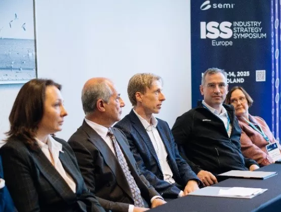
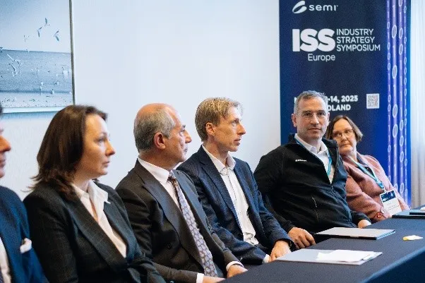
Insights from the ISS Europe 2025 Press Briefing in SopotAt the SEMI Industry Strategy Symposium Europe (ISS Europe) 2025, held in Sopot, Poland, senior leaders from government, industry, and the investment community came together to share insights on Europe’s evolving semiconductor landscape. During a dedicated press briefing, they addressed Poland’s growing role in the ecosystem, the significance of international collaboration, and the strategic levers needed to bolster Europe’s competitiveness in semiconductors.Against the backdrop of accelerating investment through the EU Chips Act, speakers emphasized that building Europe’s semiconductor future will require more than funding. It will demand cross-border collaboration, cohesive public-private strategies, and a long-term vision to ensure talent pipelines and supply chain resilience.The briefing featured remarks and commentary from:Laith Altimime, President, SEMI EuropeAgnieszka Sygitowicz, President, The Polish-Taiwanese Chamber of Commerce and IndustryPawel Pudlowski, Ph.D., Deputy CEO, Polish Investment and Trade Agency (PAIH)Monika Morali-Majkut, Chairwoman of the Supervisory Board, Atlas WardBenedikt Ernst, Senior Vice President and Head of Strategy Transformation, Merck KGaA, Darmstadt, GermanyDionys van de Ven, President, Comet YxlonAnna-Riikka Vuorikari-Antikainen, Chief Commercial Officer, Okmetic From left to right: Agnieszka Sygitowicz, President, The Polish-Taiwanese Chamber of Commerce and Industry; Pawel Pudlowski, Ph.D., Deputy CEO, Polish Investment and Trade Agency; Monika Morali-Majkut, Chairwoman of the Supervisory Board, Atlas Ward; Laith Altimime, President, SEMI Europe; Benedikt Ernst, Senior Vice President and Head of Strategy Transformation, Merck KGaA, Darmstadt, Germany; Dionys van de Ven, President, Comet Yxlon; Anna-Riikka Vuorikari-Antikainen, Chief Commercial Officer, OkmeticSEMI: How are the private sector and international partners contributing to Poland’s ecosystem development?Morali-Majkut: The private sector is essential to building Poland’s semiconductor ecosystem. At Atlas Ward, together with like-minded companies, we’ve launched SEMICON Supply Poland to help develop a strong, scalable supply chain. We’re working to ensure that essential infrastructure is ready: land, utilities, materials, and specialized service providers that can meet the needs of incoming semiconductor investments. But this isn’t just a national effort. We’re closely aligned with ecosystem-building in Dresden, Prague, and across Central Europe. Collaboration across borders is essential.Sygitowicz: We believe strongly in the philosophy of “building bridges.” In our work with Taiwan and other partners, we focus on five “bridges”: knowledge, people, business, development, and shared success. These connections are critical for Poland to become an integral part of the global semiconductor supply chain. Poland is not trying to replicate what others have done, but to learn from it—particularly in ecosystem development. The long game is not just investment attraction; it’s ecosystem maturity. SEMI: Talent shortages remain a major concern across the industry. What steps are being taken to prepare the future-ready workforce?Morali-Majkut: We are working closely with academia to build the talent pipeline Poland will need as its semiconductor sector grows. Together with industry partners, we’re developing vocational training programs and university-level collaborations aimed at aligning skills with industry needs. There are already several R D-focused projects underway at Polish technical universities, and Poland’s strong foundation in technical education positions us well to support workforce growth as the industry scales up.The semiconductor industry has one of the most complex supply chains in the world. Investing in this industry creates ripple effects across a wide range of skill areas. When we invest in semiconductor education, the spillover benefits for the broader economy will be immense.Altimime: While the talent shortage is certainly a challenge, it also presents a massive opportunity. At SEMI, we’re committed to making Europe’s semiconductor investment a long-term success. Through strong collaboration with the European Commission and a broad network of consortium partners across Europe, including Poland and other Eastern European countries, we’re pushing forward both public and private sector engagement to ensure the continuity of growth and innovation.Europe is projected to face a shortage of 271,000 skilled workers in the semiconductor sector by 2030 if current trends persist. To address this challenge, SEMI is leading a range of initiatives focused on reskilling, upskilling, and cross-sector knowledge development. We’ve established an Educational Leaders Board with 18 consortium members and are organizing events to reach out to students and educational institutions – including the recent SEMI On Campus with the University of Gdańsk — all to foster stronger connections between academia and industry. SEMI: How can Europe strengthen its semiconductor supply chain resilience in the face of geopolitical challenges?Ernst: Resilience starts with recognizing and building on Europe’s existing strengths. While much attention is often given to gaps, Europe already has world-class players, technologies, and a strong consumer market. These are key strategic assets. What’s needed now is coordination—government and industry must work together to align efforts, avoid fragmentation, and ensure that political initiatives channel support in a unified direction.Van de Ven: For industry, true resilience means the freedom to operate globally. Trade controls and IP restrictions can create bottlenecks, so policies must support open access to markets across regions—including the U.S., Europe, and Asia. Companies also need to co-create with fabs and universities, embedding themselves where talent is trained and where innovation happens. This creates a robust, future-ready ecosystem. Location decisions are increasingly influenced by proximity to both production facilities and research institutions.Sygitowicz: Poland is well-positioned to support investment through a combination of ready-to-develop land, financial incentives (such as grants and tax exemptions), and ecosystem services. Beyond infrastructure, there is growing government support for talent development and innovation. Startups, accelerators, and academic partnerships are playing a larger role in building the technology pipeline—creating a more comprehensive, innovation-friendly environment for foreign investors.Vuorikari-Antikainen: Speed is an often overlooked but critical factor in competitiveness. Europe has historically moved slowly, but if countries like Poland can create fast-track pathways for permitting, investment, and project execution, they can set themselves apart. Pairing this agility with strong education and startup ecosystems will help deliver long-term resilience and responsiveness to market needs.Altimime: We must avoid country-centric thinking. Europe’s strength lies in its diversity with different regions excel in different areas, and the challenge is to bring those strengths together. Initiatives like the pilot lines are a great example of this in action, connecting capabilities in photonics, advanced packaging, and quantum technologies across the continent. With strong leadership from Europe’s research and technology organizations (RTOs), such as the Technical Research Centre of Finland (VTT), we’re seeing renewed momentum in areas where Europe has historically been strong, like communications and photonics.To truly accelerate Europe’s position in the global semiconductor landscape, we need to focus on integration—connecting the dots between regions, institutions, and industries. From left to right: Laith Altimime, President, SEMI Europe; Benedikt Ernst, Senior Vice President and Head of Strategy Transformation, Merck KGaA, Darmstadt, Germany; Dionys van de Ven, President, Comet Yxlon; Anna-Riikka Vuorikari-Antikainen, Chief Commercial Officer, OkmeticSEMI: With the European Commission discussing a potential second Chips Act, what lessons should we carry forward from the first—and how can Poland play a stronger role?Van de Ven: The primary objective of the Chips Act should be to enable investment and industrial action. In some cases, we’ve seen frameworks become overly complex, attempting to define platforms or outcomes in ways that don’t always align with business needs. From an industry standpoint, what’s most helpful is straightforward support—mechanisms that empower companies to invest where it makes sense and move quickly. Ultimately, the private sector will determine how to build and scale the necessary infrastructure and innovation.Pudlowski: It’s true that Poland did not benefit from the first Chips Act to the extent that its assets and potential might suggest. We offer a combination of engineering talent, geographic advantage, and industrial readiness—yet, in terms of EU-level influence and visibility, we’ve been underrepresented. That is beginning to change.Poland now has a national semiconductor strategy backed by the government, and this, combined with growing engagement from organizations like SEMI, positions us for stronger inclusion going forward. At the same time, we need more bottom-up visibility. Companies in Poland should proactively present their capabilities and publish their work more widely. We have a great deal to offer, and now is the time to ensure that’s recognized in Brussels and across Europe.Altimime: Poland’s recent release of its national chip strategy is both timely and critical. From SEMI’s perspective, this is a proven model: a clear strategic roadmap, strong government backing, and industry alignment create the right environment for success. The first Chips Act delivered real progress and global attention, and with Poland’s new strategy in place, we expect to see even greater integration into the European semiconductor value chain in the next phase of the initiative.Morali-Majkut: During recent conversations with international partners, particularly in Asia, it became clear that while countries like Germany and the Czech Republic are well known within the semiconductor ecosystem, Poland has not always been equally visible—despite being geographically and industrially well-positioned. That perception is starting to shift.Poland has long played a vital role in Europe’s industrial supply chain, particularly in collaboration with Germany. We bring a strong foundation in engineering, education, cost-efficiency, and industrial land availability. These assets are highly relevant to semiconductor expansion. Rather than seeing countries in isolation, we should frame this as a collaborative regional model—linking Germany, the Czech Republic, and Poland as an integrated supply chain hub. SEMI ContactSitong He, Communications ManagerEmail: [email protected]
Read More
New pilot lines offer European innovators access to the most advanced semiconductor technologies for product development and validation.The global semiconductor landscape has undergone significant transformation in recent years. With disruptions such as the semiconductor supply chain crisis and the challenges it posed to the automotive sector, Europe’s dependence on external fabrication facilities, particularly in Taiwan, has become a pressing concern. In response, the European Union (EU) introduced the EU Chips Act, a comprehensive framework designed to reduce this reliance and boost Europe’s share of the global semiconductor market. ITF Chip into the Future, hosted by imec at SEMICON Europa 2024, was a pivotal event that brought together industry leaders, policymakers, and experts to explore the implementation of the EU Chips Act and the future of Europe’s semiconductor ecosystem. Jari Kinaret, Executive Director of the Chips Joint Undertaking (Chips JU)—the body overseeing the EU’s semiconductor investments—explained, “The Chips JU is about capacity building to drive semiconductor innovation in Europe. We will continue to be dependent on the rest of the world, but we want to make sure that the rest of the world depends on us as well.” Jari Kinaret, Executive Director, Chips JUEuropean research is driving progress towards sub-nanometer fabricationOne of the pilot lines, located at imec’s research center in Belgium, is focused on advancing methods that push Moore’s Law forward by achieving smaller and more efficient circuit features. As Luc Van den hove, President and CEO of imec, explained, “imec is now powering innovation for tomorrow’s chip designs, including stacked layers of chips, with each layer containing specific functionality implemented on chip processes optimized for each function. This allows us to scale much further than if all functionality had to be implemented on a single monolithic layer.”Luc Van den hove, President and CEO, imec Another pilot line, based in France and operated by CEA-Leti, is focused on pushing the limits of technology across multiple dimensions. CEA-Leti CEO, Sébastien Dauvé, explained that the goal of the FAMES pilot line is to advance “not only FD-SOI at 10nm and 7nm nodes, but also novel non-volatile memory technologies, RF components, 3D integration, and the development of small inductors for DC-DC converters.” Sébastien Dauvé, CEO, CEA-LetiAdvancements in 3D integration and chiplet technologies are closely tied to innovation in chip packaging. Christoph Kutter, Executive Director of Fraunhofer EMS, described how the Advanced Packaging and Heterogeneous Integration for Electronic Components and Systems (APECS) pilot line in Germany is designed to meet the needs of industrial customers’ growing demand for advanced packaging solutions. Kutter noted “Customers told us that they needed to integrate logic and power, sensors and logic, and other combinations of functions. We have built the APECS pilot line to provide what they asked for.”Christoph Kutter, Executive Director, Fraunhofer EMSThe EU Chips Act is spurring investments not only in chip fabrication but also in the underlying technologies which support chipmaking. Emmanuel Sabonnadière, EVP at Soitec, highlighted how fabrication of advanced silicon carbide (SiC) power devices “is enabled by SmartSiC™ technology from Soitec – part of a built-in-Europe solution for silicon carbide.” Sabonnadière explained that SmartSiC technology “creates very thin layers of SiC material which make really differentiated substrates supporting the production of high-performance SiC devices.” Emmanuel Sabonnadière, EVP, SoitecInnovation in materials emerged as an important theme at ITF Chip into the Future. Julien Arcamone, Vice President of Corporate R D at ASM, described the critical role of materials for atomic layer deposition (ALD) in the advancing 3D semiconductor integration. Arcamone emphasized the importance of collaboration across the semiconductor value chain, describing ASM’s partnership with imec as part of “a win-win ecosystem.” Julien Arcamone, Vice President of Corporate R D, ASMDeveloping the skills to implement advanced semiconductor technologiesWhile the EU Chips Act is subsidizing the construction of new facilities including pilot lines needed for the hardware of the semiconductor industry’s expansion – the ITF speakers underlined the equally important “software” element of the semiconductor industry ecosystem: the knowledge and expertise of the people working in the industry. One of the biggest challenges in implementing the EU Chips Act is addressing Europe’s talent gap. Katrien Marent, Executive Vice President and Chief Marketing and Communications Officer at imec, said that the gap is in part “because students who graduate in STEM subjects are not trained in advanced semiconductor technologies.” From left to right: Katrien Marent, Executive Vice President and Chief Marketing and Communications Officer, imec; Julien Arcamone, Vice President of Corporate R D, ASM; Thomas Heurung, CEO, Siemens EDA; Frédérique Le Grevès, President STMicroelectronics France and Executive Vice President, Europe France Public Affairs, STMicroelectronics; Romano Hoofman, Director imec.IC-link, imec; and Christophe Frey, Vice-President of EU engagements Managing Director, ARM.Thomas Heurung, CEO of Siemens EDA, highlighted the need for educational reform in the electronics industry. He suggested that “we might not have the right degree-level curriculum for changing times in the electronics industry. We need to change the way that we train students at university, and we need more scope for early or mid-career training on specialist micro-curriculums aimed at a particular skill or knowledge set.”The industry also struggles to attract individuals. Frédérique Le Grevès, President of STMicroelectronics France and Executive Vice President, Europe France Public Affairs of STMicroelectronics, emphasizes the importance of rebranding the industry to attract new talent. She remarked, “The word ‘semiconductor’ itself isn't very exciting—it’s even off-putting to some. By simply changing the name of educational programs, we’ve seen significant increases in enrollment. This demonstrates the power of language in shaping perceptions and interest.”Thomas Heurung of Siemens EDA also called for a stronger emphasis on entrepreneurship, noting “there is a big contrast between Europe and the US, particularly Silicon Valley.” He explained how his company’s Cre8Ventures unit had been set up to help start-ups through the key stages of creating a successful new company, including product development, attracting funding, and bringing the product to market. Thomas Fleischmann, Program Manager at Robert Bosch, explained how the EU Chips Act has accelerated the formation of the European Semiconductor Manufacturing Company (ESMC) joint venture, in which Bosch is a key stakeholder. ESMC is building a new semiconductor fabrication plant in Dresden, dedicated to producing chips for the automotive and industrial sectors. Fleischmann emphasized that ESMC will play a crucial role in helping Europe “scale advanced technologies to high volumes at a competitive cost.”In addition, the EU Chips Act also provides a broader platform for the expansion of Europe’s deep tech capacity. This includes the creation of five pilot lines, which will offer European companies access to manufacturing capacity for prototyping at the most advanced semiconductor technology nodes.Thomas Fleischmann, Program Manager, Robert BoschITF Chip into the Future at SEMICON Europa 2024 highlighted the broad scope of the EU Chips Act – not only supporting the building of advanced fabs but also providing the foundations for technology development, production, and marketing – all aimed at supporting semiconductor innovation in Europe. SEMI ContactMaria Daniela Perez, Communications ManagerEmail: [email protected]

Read More
Leaders in the semiconductor industry are finding ways to balance rapid demand growth with strategies to mitigate the risks of geopolitical uncertainty and a complex supply chain.At the CxO Summit during SEMICON Europa, industry leaders gathered to share insights into the immense opportunities ahead for the semiconductor sector, as well as the challenges that could impede growth. Laith Altimime, President of SEMI Europe, highlighted how discussions last year centered on reaching $1 trillion in global sales by 2030. “The conversation today is about how far above $1 trillion we will be in 2030,” said Altimime. “Artificial intelligence is an amazing and exciting technology, and the semiconductor industry is at the heart of it.”Laith Altimime, President, SEMI EuropeAjit Manocha, President and CEO of SEMI, described the current state of the semiconductor industry with one word – “unprecedented.” Emphasizing quantum computing as the next growth driver after AI, Manocha urged leaders to prepare for the next landmark - $4 trillion in global sales by 2040. However, the challenges facing the industry are equally unprecedented. Manocha identified four key obstacles: geopolitical volatility, the Net Zero challenge, the competition for top talent, and supply chain disruptions. “We need to work together to solve these challenges – we need unprecedented collaboration,” he explained. Ajit Manocha, President and CEO, SEMIA European Perspective on the Industry’s ChallengesWith the CHIPS Act in the US and the European Union (EU) Chips Act, the industry is also seeing unprecedented governmental engagement. Gustav Kolbe, Acting Director of Enabling and Emerging Technologies at Directorate-General for Communications Networks, Content and Technology of the European Commission, explained that Europe had been deeply impacted by the effect of trade tensions and supply chain disruptions. “In the field of semiconductors, we realized that we cannot keep doing business as usual and expect to achieve more resilience and reduced dependence on non-European supply chains,” Kolbe said. Gustav Kolbe, Acting Director of Enabling and Emerging Technologies, DG CONNECT, European CommissionJari Kinaret, Executive Director of the Chips Joint Undertaking (Chips JU), which is responsible for implementing EU Chips Act programs, described how its projects amplify the effect of EU funding by leveraging matching contributions from member states and participating companies. “This means that our budget of €4 billion actually produces investments in the semiconductor industry of about €11 billion,” he noted. Jari Kinaret, Executive Director, Chips JUThe Chips JU funded projects are designed to position Europe at the forefront of advanced semiconductor technology. Belgium’s imec, for example, is operating a Chips JU pilot line focused on leading-edge semiconductor innovation. Luc Van den hove, President and CEO of imec, highlighted the potential for 3D integration, “We can now combine multiple chips through silicon interposers with very fast connectivity between them. This allows us to build compute platforms which are far larger than what can be made with a single silicon chip,” he explained referring to this approach as “CMOS 2.0.” However, Van den hove warned that Europe cannot achieve its goals alone, emphasizing the complex semiconductor value chain and the need for collaboration. “Self-sufficiency leads to mediocrity,” he warned, advocating for a global approach that leverages the “best of the best.”Luc Van den hove, President and CEO, imecStephan Haferl, Chief Executive Officer of Comet Group, introduced the CA20, a tool designed to improve efficiency and quality in semiconductor manufacturing. The CA20 uses advanced imaging and AI to quickly identify and address production challenges, such as defects in solder bumps, without damaging components. Now fully automated, it integrates smoothly into factory workflows, providing real-time information to help manufacturers maintain high standards and increase production yields. This innovation highlights the role of new technologies in overcoming key obstacles and driving progress in the semiconductor industry.Left to right: Isabella Drolz, Vice President Marketing Product Strategy, Comet Yxlon; Laith Altimime, President, SEMI Europe; Stephan Haferl, Chief Executive Officer, Comet Group; and Dionys van de Ven, President, Comet YxlonCarlos Mazure, Chief Strategy Officer at Institute of Microelectronics – A*STAR in Singapore, illustrated this point by highlighting the institute’s focus on advanced packaging, a key Singaporean strength. “We have built a state-of-the-art 300mm prototyping line, enabling companies to implement wafer-to-wafer and chip-to-wafer bonding as well as fanout chip packaging,” Mazure said. Carlos Mazure, Chief Strategy Officer, Institute of Microelectronics – A*STARTurning back to Europe, Pierre Barnabé, CEO of Soitec, highlighted materials science as a regional strength. Soitec’s engineered substrates are driving energy efficiency breakthroughs in electronic, acoustic, and photonic applications. “We can bond anything to anything, creating advanced substrates for any active layer,” Barnabé explained. Pierre Barnabé, CEO, SoitecKai Beckmann, Member of the Executive Board and CEO Electronics at Merck KGaA, Darmstadt, Germany, also emphasized the role of materials in enabling sustainable growth. “The semiconductor industry faces a challenge with the contribution of process gases to its total greenhouse gas emissions. We hope to solve the problem by using AI to support materials research, and to design new molecules – an approach we have learned from the pharmaceuticals industry,” Beckmann shared. Kai Beckmann, Member of the Executive Board and CEO Electronics, Merck KGaA, Darmstadt, GermanyCollaboration Strengthens the Semiconductor Supply Chain Despite the breadth of enabling technologies emerging from Europe, the rapid growth in semiconductor demand has not always been matched by a secure supply. Barbara Frenkel, Member of the Executive Board Purchase at Porsche, shared that the company is collaborating with the industry to improve its access to the chips needed for automotive electrification. This includes joining industry groups such as the SEMI Global Automotive Advisory Council (GAAC) and, as she said, “learning your language.” Frenkel added, “Porsche aims to emulate Apple’s approach with Intel and Motorola to drive innovation – we will do the same with suppliers of automotive chips.”Barbara Frenkel, Member of the Executive Board Purchase, PorscheAnother solution to supply constraints is to widen the supply pipeline. John Behnke, General Manager for Smart Manufacturing at Inficon, described how smart technology can significantly improve efficiency and output. “A semiconductor fab is 100 times more complicated than anything else in the world – it is a mathematical nightmare to model it. That gives massive opportunities for improved productivity if we can implement smart control technologies,” Behnke explained. John Behnke, General Manager for Smart Manufacturing, InficonThe Challenge of Achieving Sustainable GrowthWhile the prospect of exceeding $1 trillion in annual sales energizes the industry, there is widespread recognition that growth must not come at the expense of environmental responsibility. As the industry doubles in size in the 2020s, it cannot afford to double its use of resources, such as energy or greenhouse gas emissions. Frédéric Godemel, Executive Vice President for Power Systems and Services at Schneider Electric, shared that the biggest impact on sustainability could come from “energy frugality” – using energy more efficiently. He explained that implementing data fusion in a semiconductor fab – combining detailed analysis of the operation of chillers with external data sets, such as weather conditions to allow for more efficient use – results in energy savings of 10%. “This approach saved costs, reduced CO2 emissions, and provided a financial payback in less than one year,” Godemel said.Frédéric Godemel, Executive Vice President for Power Systems and Services, Schneider ElectricThe value of smart control in fab operations was also highlighted by Katharina Westrich, Global Vice President of Electronics, Semiconductors Simulation Digital Industries at Siemens. She described how Siemens makes digital twins of factories before they are built. “This is an approach that the semiconductor industry can also adopt,” Westrich said. “A digital twin enables more efficient allocation of resources to the fab and sub-fab, allowing simulation of fab operation and optimization of processes and resources.”Katharina Westrich, Global Vice President of Electronics, Semiconductors Simulation Digital Industries, SiemensThe semiconductor industry faces a future full of opportunity, yet also marked by significant obstacles—ones that delegates at the CxO Summit are now better equipped to tackle head-on.On behalf of SEMI, the SEMI Europe team would like to express appreciation to the industry leaders for sharing their visions and readiness to collaborate during the CxO Summit.SEMI ContactCassandra Melvin, Senior Director of Business Development and OperationsEmail: [email protected]
Read More