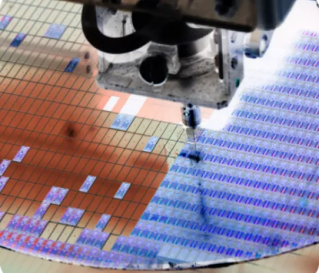


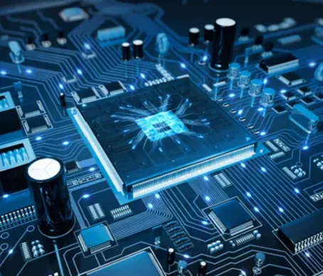
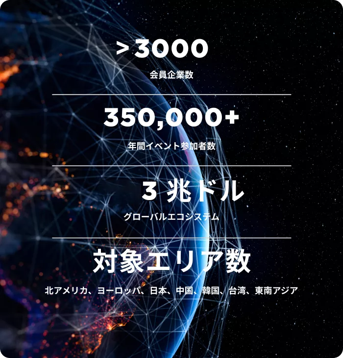
半導体サプライチェーン業界に与えるSEMIのグローバルインパクト
SEMIはマイクロエレクトロニクスをリードする工業会として、会員のビジネスを支援し、国際的な最重要課題に取り組んでいます。
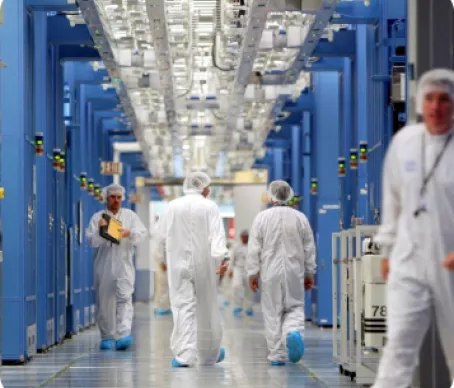
半導体産業の活性化のために


ニュースルーム
SEMIと世界の半導体産業でで起こっていることを知る。


SEMI会員特典
会員企業はSEMIの製品やサービスを通じて2022年に総計1500万ドルの費用を節約しました。
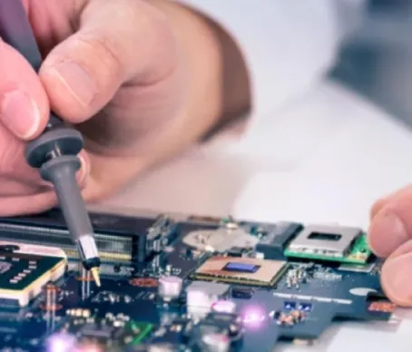
製品とサービス
SEMIスタンダードおよび市場レポートは、パートナーや競合企業間とのコラボレーションを支援し、事業の戦略的判断を容易にし、製品開発を促進します。
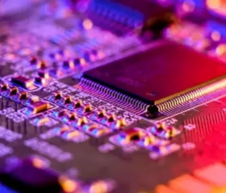
インダストリーグループ
同業者と協力して技術ギャップを特定し、集合的なソリューションを加速させ、高成長の市場セグメントを開拓します。