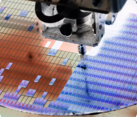


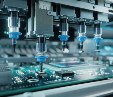
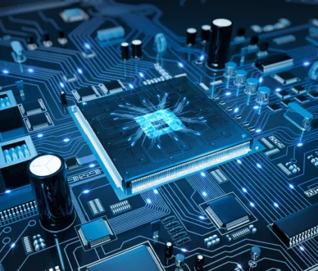
Global Impact on Semiconductor ecosystem
SEMI is the leading microelectronics industry association with programs that help members grow their business and address top challenges worldwide.


SEMI Membership
Member companies saved $15 million total in 2022 on SEMI products and services.


WHY JOIN SEMI
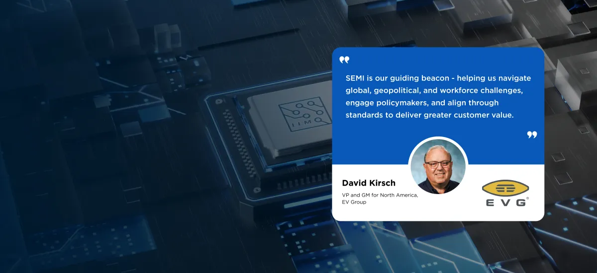
Be a part of our collective efforts to navigate geopolitical tensions, increase supply chain resilience, grow sustainably, and overcome industry challenges.

Join our member community
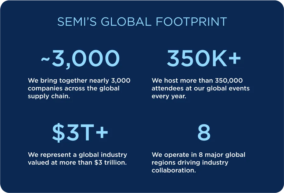
Connect with a global network of 3,000+ SEMI member companies and unlock exclusive discounts and benefits on events, communities, market data, industry standards and more.
PRODUCTS & SERVICES
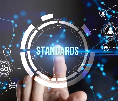
SEMI manufacturing standards and industry market reports support collaboration between partners and competitors, facilitate strategic business decisions, and accelerate product development…


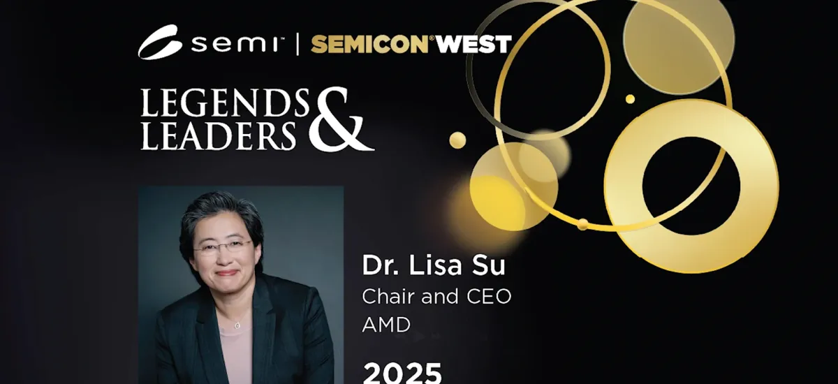
NEWSROOM
Discover what’s going on at SEMI and across the global microelectronics industry


INDUSTRY GROUPS