


SEMI對全球半導體供應鏈的影響
SEMI 為全球半導體產業協會,積極發揮第三方平台角色,推動各項發展計畫,協助會員開拓市場業務與應對產業挑戰。
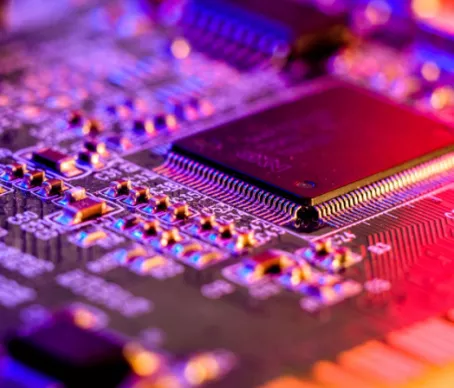
強化晶片產業


新聞中心
了解 SEMI 以及全球微電子產業最新動態


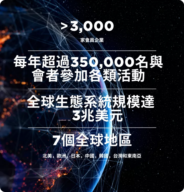
SEMI會員權益與價值
2022年,會員公司在 SEMI 產品與服務上共省了1500萬美元
產品和服務
SEMI標準和產業市場報告支持合作夥伴與競爭對手之間的協作,促進策略性決策,並加速產品開發...
產業社群
與產業合作共同解決技術端挑戰,有效地提出解決方案,推動產業未來發展